Nonvolatile semiconductor memory device

a nonvolatile, memory device technology, applied in semiconductor devices, transistors, instruments, etc., can solve the problems of low erase speed, restricted data retention characteristics, and increased chip cost, so as to improve the performance and reliability of a nonvolatile semiconductor memory device, and avoid characteristic deterioration

Active Publication Date: 2005-10-20
RENESAS ELECTRONICS CORP
View PDF8 Cites 46 Cited by
  • Summary
  • Abstract
  • Description
  • Claims
  • Application Information

AI Technical Summary

Benefits of technology

[0023] It is an object of the present invention to enhance the performance and reliability of a nonvolatile semiconductor memory device.
[0024] It is another object of the present invention to avoid characteristic deterioration that may be caused by holes accumulated by erase operations.
[0037] Further, the performance and reliability of a nonvolatile semiconductor memory device can be enhanced. Particularly, it is possible to increase the erase speed and improve the programming / erasing endurance characteristics. It is also possible to increase the read speed and improve the data retention characteristic.

Problems solved by technology

When the tunneling erase method is employed, there is a tradeoff between the data retention characteristic and erase characteristic.
However, since it is hard to have an electrical charge tunnel through a thick oxide during an erase operation, a low erase speed is lowered.
However, an increase in the erase voltage enlarges the scale of a peripheral circuit, thereby increasing the chip cost.
The oxide for electron extraction is limited to a small film thickness permitting electron tunneling so that the data retention characteristic is restricted.
Further, since electrons injected for programming are extracted for erase purposes, the threshold value prevailing after erase cannot be lowered below an initial threshold voltage at which the silicon nitride film is electrically neutral.
If the threshold value cannot be sufficiently decreased, a large read current cannot be obtained.
As a result, it is difficult to provide an increased read speed.
As a result, the repeated execution of a programming / erase operation is restricted.
Further, the accumulated holes deteriorate the charge retention characteristic.
Therefore, if the holes are excessively accumulated directly above the diffusion layer, the holes are locally accumulated even in a programming state.

Method used


Image

  • Nonvolatile semiconductor memory device
  • Nonvolatile semiconductor memory device
  • Nonvolatile semiconductor memory device

Examples


Embodiment Construction

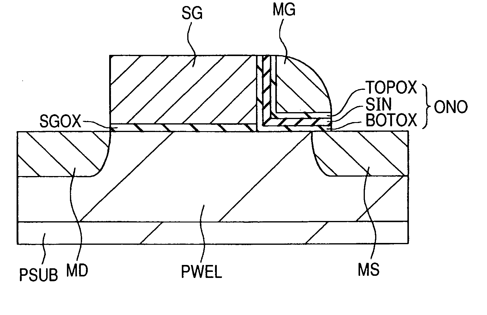
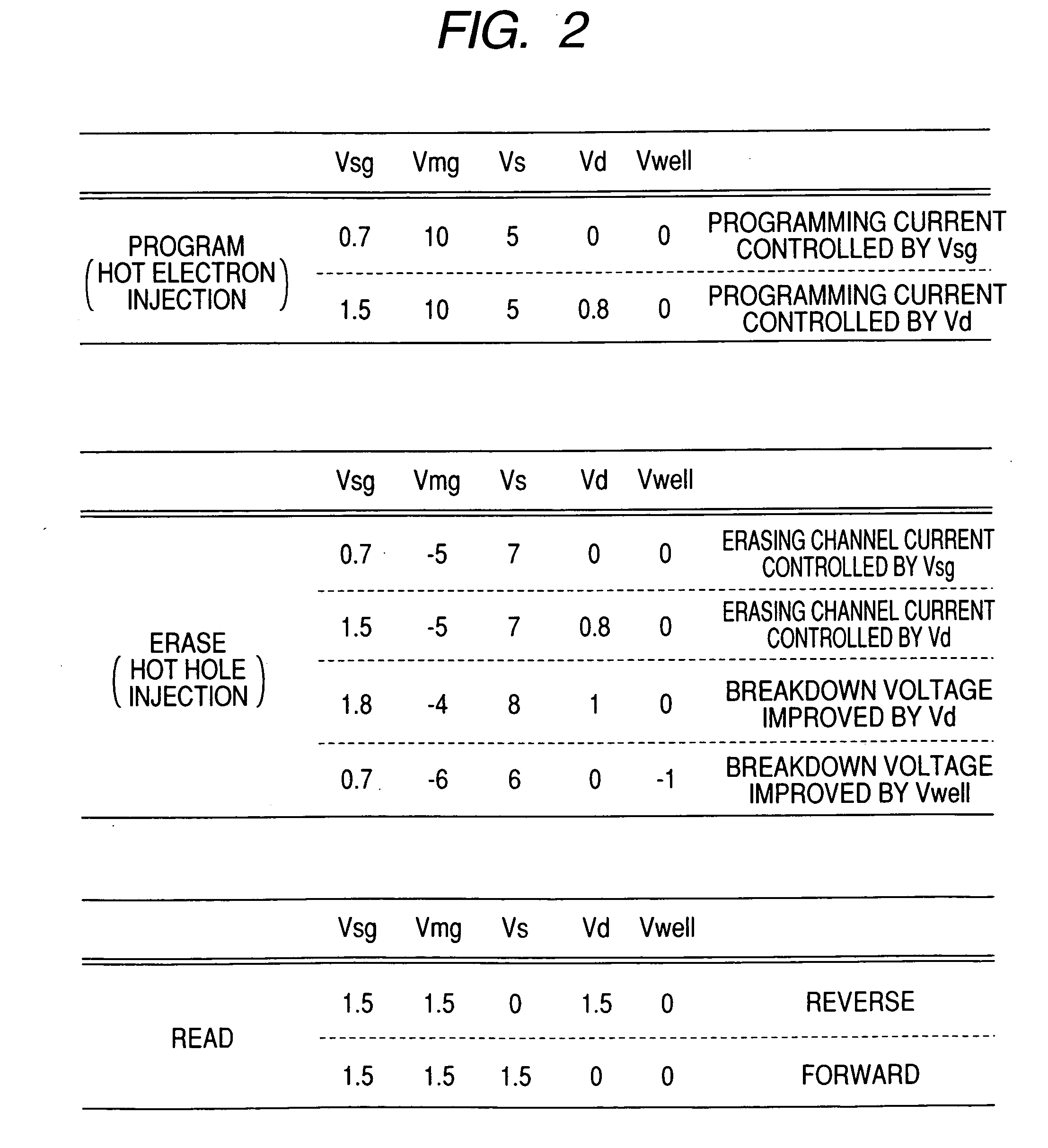
[0069] Embodiments of the present invention will now be described with reference to the accompanying drawings. Elements having the same functions are assigned the same reference numerals in all the drawings depicting the embodiments, and will not be repeatedly described. In the following description of the embodiments, identical or similar portions will not be repeatedly described unless necessary.

[0070] The present invention uses a trap type insulator (insulation film that can store an electrical charge) for a charge storage section. Therefore, the following description of the embodiments assumes the use of a memory cell that employs a trap type insulator based on an NMOS (n-channel MOS) transistor. The polarities (application voltage polarity and carrier polarity for programming, erasing, or reading) designated in the following embodiments are used in order to describe operations of a memory cell that is based on an NMOS (n-channel MOS) transistor. If the memory cell is based on ...


PUM


Abstract

In a situation where a memory cell includes an ONO film, which comprises a silicon nitride film for charge storage and oxide films positioned above and below the silicon nitride film; a memory gate above the ONO film; a select gate, which is adjacent to a lateral surface of the memory gate via the ONO film; a gate insulator positioned below the select gate; a source region; and a drain region, an erase operation is performed by injecting holes generated by BTBT into the silicon nitride film while applying a positive potential to the source region, applying a negative potential to the memory gate, applying a positive potential to the select gate, and flowing a current from the drain region to the source region, thus improving the characteristics of a nonvolatile semiconductor memory device.

Description

CLAIM OF PRIORITY [0001] The present application claims priority from Japanese application JP 2004-106850 filed on Mar. 31, 2004, the content of which is hereby incorporated by reference into this application. FIELD OF THE INVENTION [0002] The present invention relates to a nonvolatile semiconductor memory device and more particularly to a nonvolatile semiconductor memory device that is suitable for erase speed enhancement and programming endurance characteristics improvement. BACKGROUND OF THE INVENTION [0003] EEPROMs (Electrically Erasable and Programmable Read Only Memories) are widely used as a nonvolatile semiconductor memory device that is electrically erasable and programmable. These memory devices, which are represented by a widely used flash memory, have a conductive floating gate surrounded by an oxide or a trap insulator under a MOS (Metal Oxide Semiconductor) transistor gate. They use an electrical charge in the floating gate or trap insulator as stored information and r...

Claims


Application Information

Patent Timeline
Patent Type & Authority Applications(United States)
IPC IPC(8): G11C16/02G11C16/04H01L21/28H01L21/336H01L21/8247H01L27/105H01L27/115H01L29/78H01L29/788H01L29/792
CPCG11C16/0466H01L29/792H01L29/66833H01L21/28282H01L29/40117H01L29/4234
Inventor ISHIMARU, TETSUYAHISAMOTO, DIGHYASUI, KANKIMURA, SHINICHIRO
Owner RENESAS ELECTRONICS CORP
Why Eureka
Try Eureka