Non-volatile semiconductor memory device and method for producing same

a semiconductor memory and non-volatile technology, applied in the direction of semiconductor devices, electrical devices, transistors, etc., can solve the problems of no progress in voltage reduction or speed increase, the thickness of the dielectric film between the active region of the semiconductor and the gate electrode cannot be reduced to 3 nm or less, and the voltage cannot be reduced or increased. , to achieve the effect of improving the charge holding characteristic, reducing the voltage, and increasing the speed

Inactive Publication Date: 2005-10-20
SONY CORP
View PDF0 Cites 71 Cited by
  • Summary
  • Abstract
  • Description
  • Claims
  • Application Information

AI Technical Summary

Benefits of technology

[0012] A second object of the present invention is to provide a non-volatile semiconductor memory device having a charge storage layer structure capable of achieving a reduction of the voltage and increase of the speed by improving the charge holding characteristic and reducing the thickness of the bottom dielectric film while maintaining the required charge holding time and a method of producing the same.
[0013] A third object of the present invention is to provide a non-volatile semiconductor memory device having a charge storage layer structure not reducing the amount of charge traps from a state immediately after formation by sealing in the hydrogen and suppressing the aging of the device characteristics and a method of producing the same.

Problems solved by technology

In a conventional MONOS type memory transistor having a charge storage layer made of a single silicon nitride film or silicon oxynitride film, there was a problem that the thickness of the bottom dielectric film could not be reduced to 3 nm or less since the required charge holding time was ensured.
Further, the thickness of the dielectric film between the semiconductor active region and the gate electrode can not be reduced by a silicon dioxide conversion, so there was the problem that no progress was made in reduction of the voltage or an increase of the speed.
Consequently there was a possibility of occurrence of aging of the device characteristics.

Method used


Image

  • Non-volatile semiconductor memory device and method for producing same
  • Non-volatile semiconductor memory device and method for producing same
  • Non-volatile semiconductor memory device and method for producing same

Examples


first embodiment

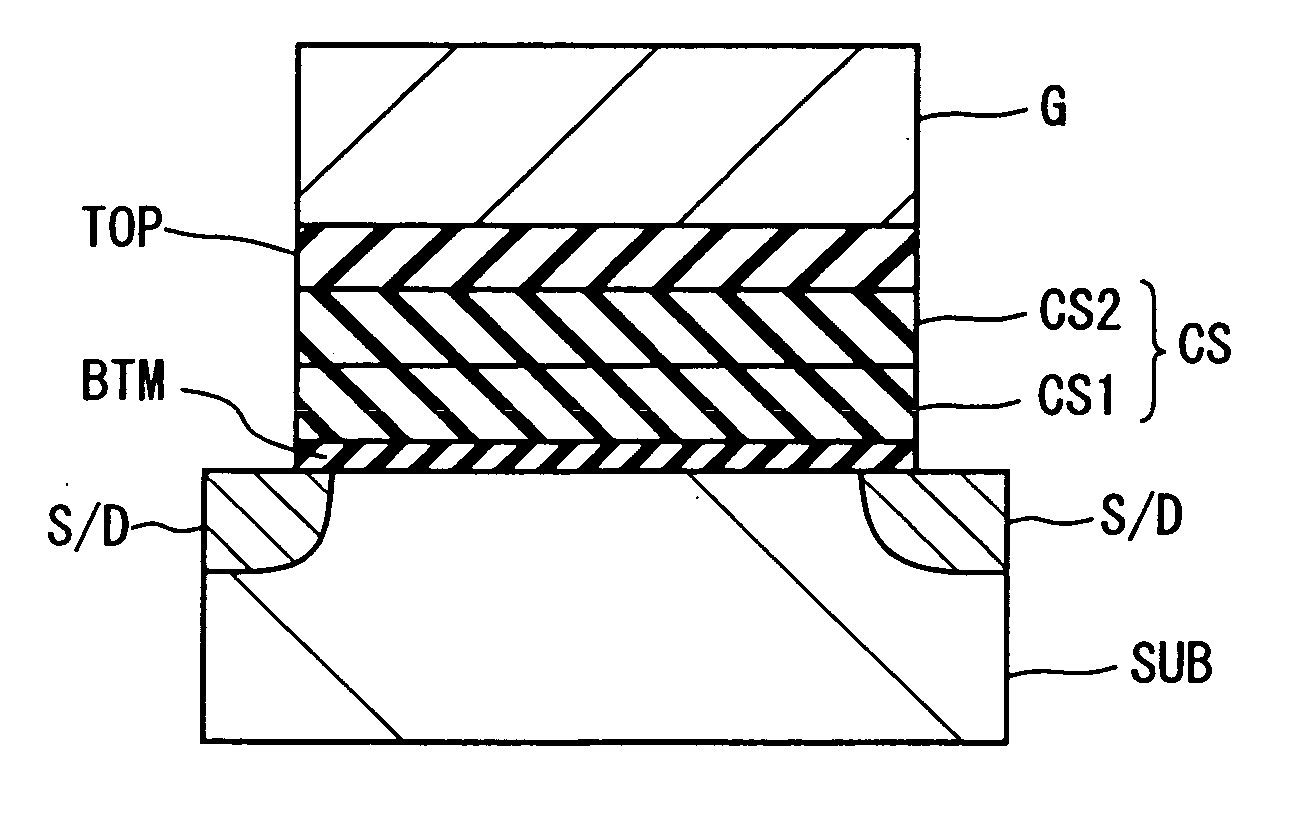
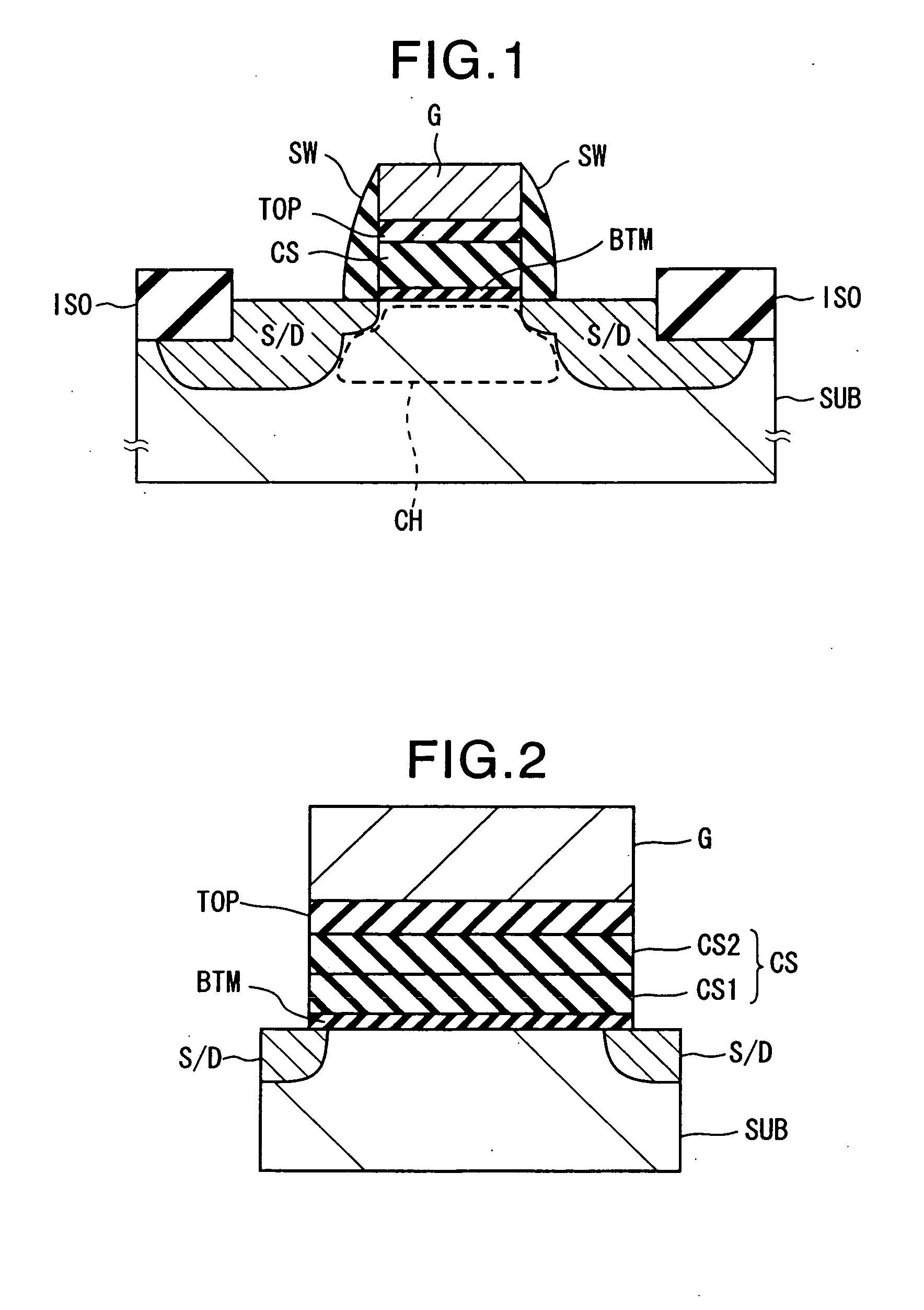
[0030]FIG. 1 shows an example of the sectional structure of the non-volatile memory transistor according to the first embodiment. Further, FIG. 2 is a view showing enlarged a principal part of FIG. 1 showing a detailed example of the structure of the charge storage layer.

[0031] This memory transistor is formed on for example a p-type silicon wafer or other semiconductor substrate, a p-well formed on the surface inside a semiconductor substrate, or a p-type silicon layer of an SOI type substrate isolation structure (hereinafter simply referred to as a “substrate SUB”). Dielectric isolation layers ISO formed by for example LOCOS (local oxidation of silicon) or STI (shallow trench isolation) is formed on the surface of the substrate SUB according to need. The substrate surface portion on which the dielectric isolation layers ISO are not formed becomes the active region on which the element containing the related memory transistor is to be formed.

[0032] On the active region are stacke...

second embodiment

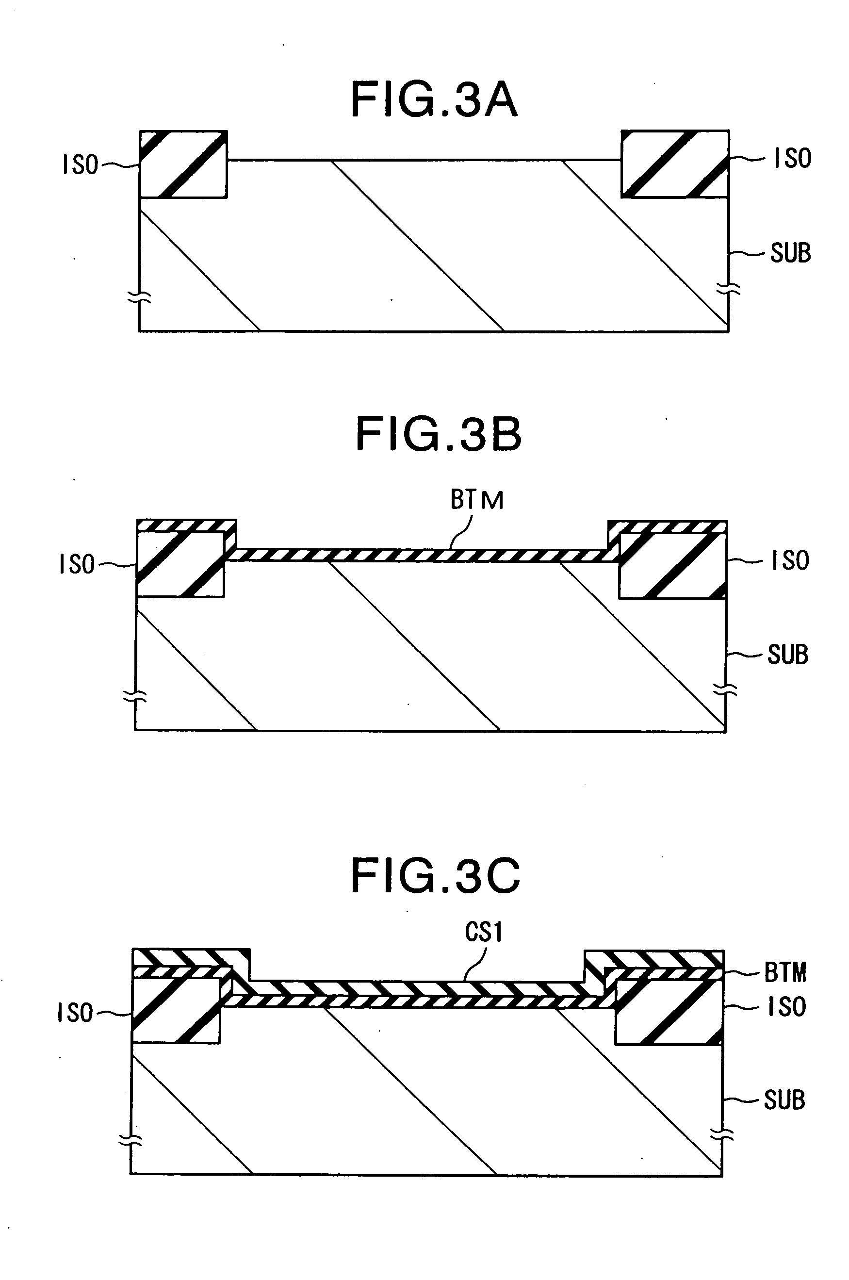
[0096] In the method of producing the memory transistor according to the second embodiment, the same steps are carried out in the same way as the first embodiment up to the formation of the first nitride film CS1 of FIG. 3A to FIG. 3C.

[0097] In the formation of the second nitride film CS2 of FIG. 3D, CVD of silicon nitride is carried out by passing monosilane SiH4 and ammonia NH3 by predetermined flow rates within a range of from 10 sccm to 500 sccm and under a condition that the pressure in the chamber becomes several hundreds of mTorr while holding the substrate temperature the same as that at the time of formation of the first nitride film CS1 or changing it according to need within a range of from 600° C. to 800° C. When the CVD is stopped after the elapse of a predetermined time, a silicon nitride film (second nitride film CS2) of several nm is formed on the first nitride film CS1.

[0098] Thereafter, by a similar method to that of the first embodiment, the various steps of the...

third embodiment

[0099] In the method of producing a memory transistor according to the third embodiment, the same steps are carried out in the same way as the first embodiment up to the formation of the first nitride film CS1 of FIG. 3A to FIG. 3C.

[0100] In the formation of the second nitride film CS2 of FIG. 3D, CVD of silicon nitride is carried out by passing silane trichloride SiHCl3 and ammonia NH3 by predetermined flow rates within a range from 10 sccm to 500 sccm and under a condition that the pressure in the chamber becomes several hundreds of mTorr while holding the substrate temperature the same as that at the time of formation of the first nitride film CS1 or changing it according to need within a range of from 600° C. to 800° C. When the CVD is stopped after the elapse of a predetermined time, a silicon nitride film (second nitride film CS2) of several nm is formed on the first nitride film CS1.

[0101] Thereafter, by a similar method to that of the first embodiment, the various steps of...


PUM


Abstract

The memory device has a plurality of dielectric films including charge storage layers CS having a charge holding capability therein and stacked on an active region of a semiconductor SUB and electrodes G on the plurality of dielectric films. Each charge storage layer CS includes a first nitride film CS1 made of silicon nitride or silicon oxynitride and a second nitride film CS2 made of silicon nitride or silicon oxynitride and having a higher charge trap density than the first nitride film CS1. The first nitride film CS1 is formed by chemical vapor deposition using a first gas which contains a first silicon-containing gas containing chlorine with a predetermined percent composition and a nitrogen-containing gas as starting materials. The second nitride film CS2 is formed by chemical vapor deposition using a second gas which contains a second silicon-containing gas having a lower chlorine percent composition than the above predetermined percent composition and a nitrogen-containing gas as starting materials.

Description

TECHNICAL FIELD [0001] The present invention relates to a structure and method of fabrication of a charge storage layer of a non-volatile semiconductor memory device as represented by a flash EEPROM (flash electrically erasable and programmable ROM). BACKGROUND ART [0002] Information is held in a non-volatile semiconductor memory transistor by storing a charge in a layer of for example polycrystalline silicon sandwiched between silicon dioxide or silicon nitride sandwiched between silicon dioxide on a semiconductor active region in which a channel is to be formed (hereinafter referred to as a “charge storage layer”). [0003] Realization of a sufficient charge holding time becomes possible by making the silicon dioxide film on the semiconductor active region side (bottom dielectric film) thick. In general, a bottom dielectric film in an FG (floating gate) type using polycrystalline silicon as the charge storage layer must be formed to at least about 10 nm, while a bottom dielectric fi...

Claims


Application Information

Patent Timeline
Patent Type & Authority Applications(United States)
IPC IPC(8): H01L21/28H01L21/318H01L21/8247H01L21/762H01L27/115H01L27/12H01L29/788H01L29/792
CPCH01L21/28282H01L29/792H01L21/7624H01L29/40117
Inventor NOMOTO, KAZUMASAAOZASA, HIROSHIFUJIWARA, ICHIROTANAKA, SHINJI
Owner SONY CORP
Why Eureka
Try Eureka