Light emitting device, manufacturing method thereof, and electronic apparatus

a technology manufacturing methods, applied in the direction of static indicating devices, discharge tubes luminescnet screens, instruments, etc., can solve the problems of light emitting element life decay or shorter life, and achieve the effect of improving the reliability of light emitting devices

Active Publication Date: 2005-10-20
SEMICON ENERGY LAB CO LTD
View PDF27 Cites 58 Cited by
  • Summary
  • Abstract
  • Description
  • Claims
  • Application Information

AI Technical Summary

Benefits of technology

[0031] According to the sealing structure and the element structure of the invention, reliability of a light emitting device can be improved significantly.

Problems solved by technology

An EL material that forms an EL layer deteriorates quite easily resulting from oxidation or moisture absorption due to oxygen or moisture, which leads to a luminance decay or shorter life of the light emitting element.

Method used


Image

  • Light emitting device, manufacturing method thereof, and electronic apparatus
  • Light emitting device, manufacturing method thereof, and electronic apparatus
  • Light emitting device, manufacturing method thereof, and electronic apparatus

Examples


embodiment mode 1

[Embodiment Mode 1]

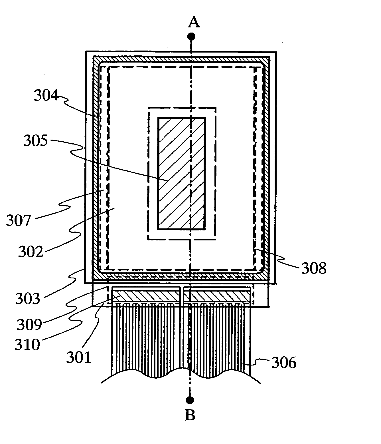
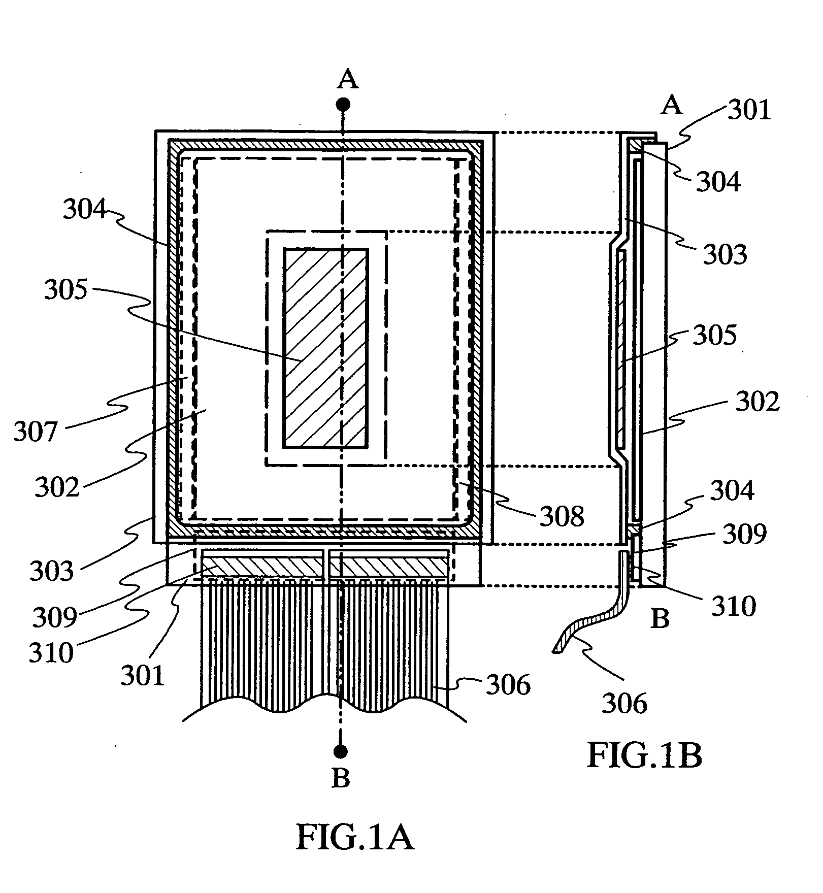
[0047]FIGS. 1A and 1B illustrate an example of a connection structure between a light emitting device and an FPC, and a sealing structure of the light emitting device respectively.

[0048]FIG. 1A is a top view of a light emitting device, and FIG. 1B is a cross-sectional view along a chain line A-B in FIG. 1A.

[0049] As shown in FIGS. 1A and 1B, according to the invention, a pixel portion 302 and a peripheral circuit portion 309 are formed on a common substrate, and a terminal electrode 310 for connection to an FPC 306 is provided above TFTs of the peripheral circuit portion. By disposing the terminal electrode 310 in the space where the peripheral circuit portion 309 is disposed, reduction in frame portion can be achieved.

[0050] In addition, since a covering material 303 is firmly fixed by use of a sealant 304 that is in contact with an edge and periphery of the substrate, the distance between the pixel portion 302 and the edge of the substrate, namely the frame p...

embodiment mode 2

[Embodiment Mode 2]

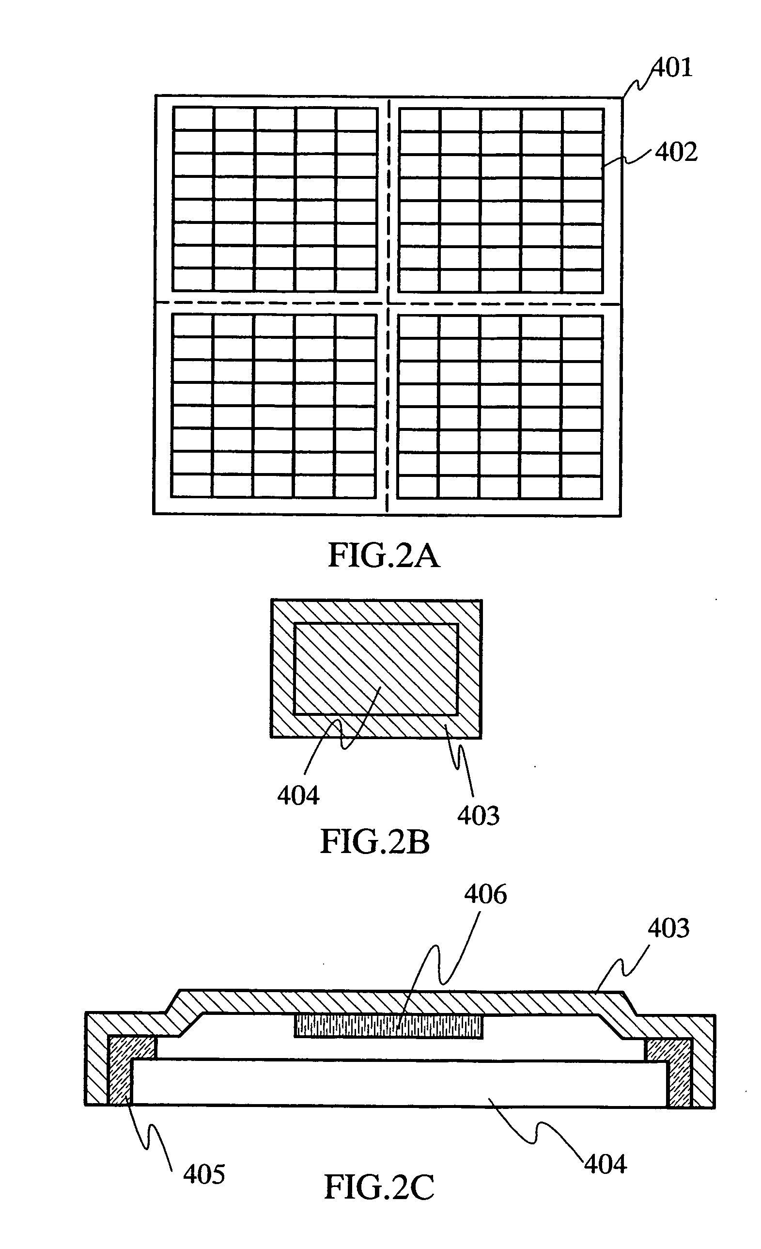
[0093]FIG. 5 illustrates an example of a full color light emitting device where the reliability of RGB light emitting elements differs from each other. Here, only a light emitting area of a light emitting element that has lower reliability than the light emitting elements of the other colors is enlarged.

[0094]FIG. 5 is a layout where a plurality of light emitting elements each having stacked layers of a first electrode, an organic compound layer on the first electrode and a second electrode on the organic compound layer are arranged. FIG. 5 corresponds to the layout where the manufacture of a TFT and a first electrode is completed.

[0095]FIG. 9E corresponds to an equivalent circuit diagram of the pixel layout diagram shown in FIG. 5.

[0096] In FIG. 5, a first electrode 801 of a blue light emitting element is formed larger than a first electrode 802 of a green light emitting element and a first electrode 803 of a red light emitting element.

[0097] In addition, a b...

embodiment 1

[0108] In this embodiment, description is made with reference to FIGS. 6A to 61 on the illustrative manufacturing steps of a semiconductor layer where crystallization of doping metal elements is performed, oxidation is performed by use of an ozone-containing solution, heat treatment is performed for reducing distortions, and then gettering is performed.

[0109] In FIG. 6A, reference numeral 710 denotes a substrate having an insulating surface, 711 denotes an insulating film to serve as a blocking layer, and 712 denotes a semiconductor film having an amorphous structure.

[0110] First, as shown in FIG. 6A, the base insulating film 711 made of an insulating film such as a silicon oxide film, a silicon nitride film and a silicon oxynitride film (SiOxNy) is formed over the substrate 710.

[0111] Then, the first semiconductor film 712 having an amorphous structure is formed over the base insulating film. The first semiconductor film 712 is formed of a semiconductor material containing silic...


PUM


Abstract

Further reduction in frame portion is achieved in the case where a driver circuit and a pixel portion are formed on a common substrate. Also, a light emitting device is provided with an advantageous structure for obtaining a large number of panels by use of a large substrate, whereby the number of panels taken out from a substrate can be increased, leading to better productivity. According to the invention, a terminal electrode is provided in the position overlapping a peripheral circuit portion, and the terminal electrode is connected to an FPC with an anisotropic conductive adhesive material. In addition, a covering material is firmly fixed by using a sealant that is in contact with the edge and periphery of a substrate.

Description

BACKGROUND OF THE INVENTION [0001] 1. Field of the Invention [0002] The present invention relates to an organic light emitting element comprising an anode, a cathode and a layer containing an organic compound that can obtain light emission when an electric field is applied thereto (hereinafter referred to as an “organic compound layer”, an “electroluminescent layer” or an “EL layer”), and a light emitting device using such an organic light emitting element. For example, the invention relates to an electronic apparatus mounting as its component a light emitting device that includes an organic light emitting element. [0003] Note that the light emitting device in this specification refers to an image display device, a light emitting device or a light source (including a lighting system). In addition, a module where a connector such as a Flexible Printed Circuit (hereinafter referred to as a FPC), a TAB (Tape Automated Bonding) tape and a TCP (Tape Carrier Package) is attached to a ligh...

Claims


Application Information

Patent Timeline
Patent Type & Authority Applications(United States)
IPC IPC(8): G09G3/30H01L27/32H01L51/52H05B33/02H05B33/06H05B33/10H05B33/14H05B44/00
CPCH01L51/5246H01L27/3276H01L51/524H10K59/131H10K50/841H10K50/8426
Inventor YAMAZAKI, SHUNPEIOSAME, MITSUAKIKOYAMA, JUN
Owner SEMICON ENERGY LAB CO LTD
Why Eureka
Try Eureka