Chip-type sensor against ESD and stress damages and contamination interference

a sensor and chip technology, applied in the direction of resistance/reactance/impedence, instruments, measurement devices, etc., can solve the problems of inability to withstand esd damage or force impingement, inability to resist esd damage or stress damage, and inability to crack, so as to effectively avoid contamination interference, enhance the sensing effect of the sensor, and prolong the life of the sensor

Active Publication Date: 2005-10-20
XIANGQUN SCI & TECH
View PDF6 Cites 86 Cited by
  • Summary
  • Abstract
  • Description
  • Claims
  • Application Information

AI Technical Summary

Benefits of technology

[0016] It is therefore an object of the invention to provide a chip-type fingerprint sensor against the ESD and stress damages and effectively avoiding the contamination interference so as to enhance the sensing effect of the sensor and lengthen the lifetime thereof.
[0017] To achieve the above-mentioned object, the invention provides a chip-type sensor against ESD and stress damages and contamination interference. The chip-type sensor includes a substrate structure and a protection layer covering over the substrate structure. The protection layer includes, from bottom to top, a first layer for providing a first stress against the substrate structure, a second layer for providing a second stress against the substrate structure, and a third layer for providing a third stress against the substrate structure. The first stress and the third stress belong to one of a tensile stress and a compressive stress, and the second stress belongs to the other of the tensile stress and the compressive stress so as to reduce the residual stress.

Problems solved by technology

However, when the hard layer is formed on the substrate structure using the semiconductor processing method, the thickness limitation thereof will be encountered because of the residual thermal stress between the hard layer and the substrate structure.
If the hard layer is thick, it tends to crack owing to the stress.
Consequently, the chip tends to crack and cannot withstand the ESD damage or force impingement.
Nevertheless, a relatively large residual thermal stress still exists therein, which will induce material defects therein and form stress concentration points around those defects, and may easily be broken by external force or ESD.
Also, because the structure of the protection layer of the above-mentioned patents cannot be effectively increased in thickness, the protection against the ESD damage cannot be achieved only depending on the material property of the protection layer.
However, the key issues having to be considered is the process and material compatibility when implementing the exposed metal mesh on the fingerprint sensor chip to solve the ESD problem.
However, the used manufacturing processes, the single layer TiN serving as the metal sense electrode material, and the exposed metal mesh material is not a standard processing step in commercial IC foundry.
In addition, the thin TiN film may have the step coverage problem when it is formed on the rugged chip surface.
Furthermore, because of the high resistivity of the TiN film, an arbitrarily large current caused by the electrostatic charges flowing therethrough may burn it out due to the joule heating effect.
However, the manufacturing processes cannot be compatible with the silicon IC manufacturing processes because the gold material may cause contamination.
However, in the step of depositing the tungsten metal and the subsequent etching back step, small cavities, which are regarded as defects and cause the problems such as stress concentration points around those defects, are formed on the sensor surface of the protection layer of silicon carbide.
When the fingernail unintentionally hits the external surface of the sensor, the sensor may be damaged.
Furthermore, the small cavities make the surface of the protection layer hydrophilic.
Thus, the moisture of the finger tends to diffuse after the finger contacts the external surface, and the image quality is deteriorated accordingly.
However, this way makes the manufacturing processes too complicated and is not suitable for the general manufacturing procedures of the commercial IC foundry.
Furthermore, when the above-mentioned technology is implemented in the capacitive fingerprint sensor, the protection layer material (the materials of the above-mentioned protection layers have the hydrophilic or lipophilic property) cannot prevent the finger's grease or sweat forming a latent fingerprint thereon after moving the finger from the sensor surface.

Method used


Image

  • Chip-type sensor against ESD and stress damages and contamination interference
  • Chip-type sensor against ESD and stress damages and contamination interference
  • Chip-type sensor against ESD and stress damages and contamination interference

Examples


first embodiment

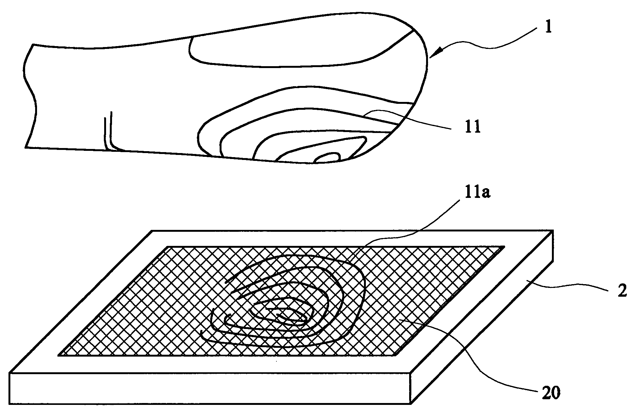
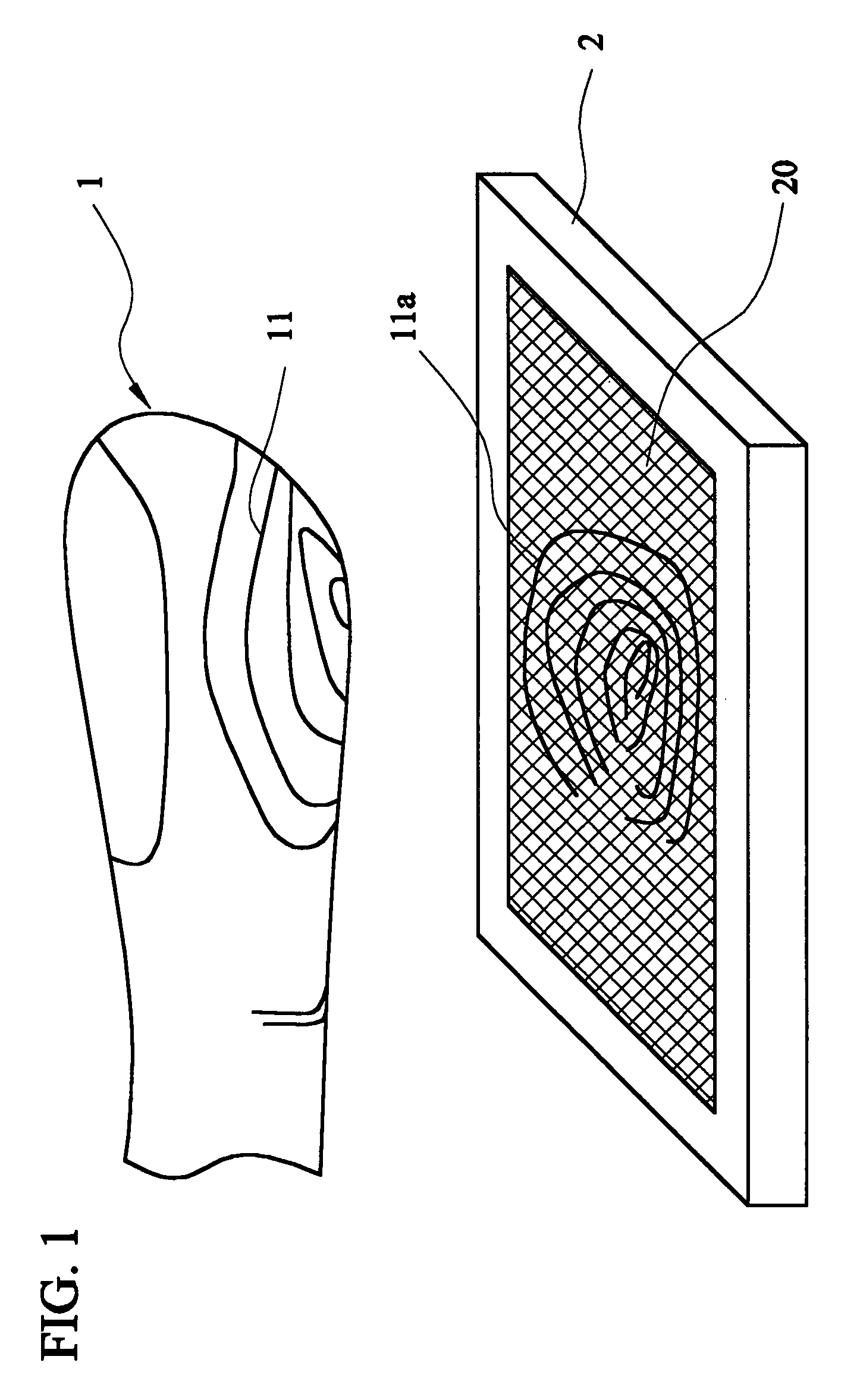
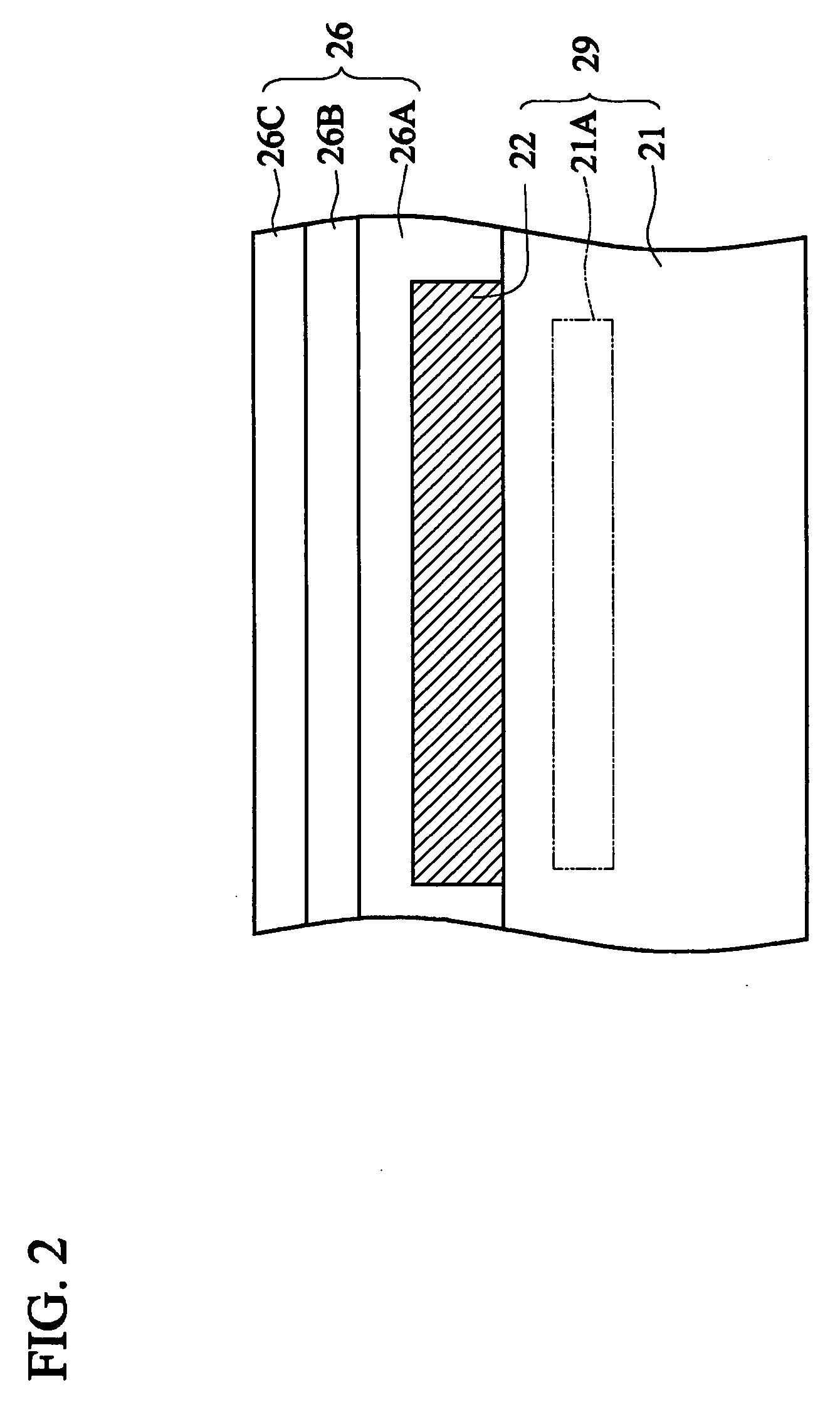
[0030]FIG. 2 is a partially schematic side view showing a capacitor sensing member of FIG. 1 according to the invention. As shown in FIG. 2, the capacitive fingerprint sensor of the invention includes a silicon substrate 21, a plurality of sense electrodes 22 (only one electrode is shown in the drawing), and a protection layer 26. The silicon substrate 21 contains a sense circuit 21A corresponding to each sense electrode 22, and includes a signal processing / control circuit 21B (schematically shown in FIG. 4) around the sensing member array, wherein the detailed arrangements of the sensing member array and the peripheral circuit may be found in the above-mentioned disclosure entitled “CAPACITIVE FINGERPRINT SENSOR”. The sense electrode 22 is positioned on the silicon substrate 21 and is electrically connected to the sense circuit 21A, wherein the portion below the sense electrode 22 and including the sense circuits 21A, the signal processing / control circuit 21B, and the silicon subst...

second embodiment

[0035]FIG. 3 is a partially schematic side view showing the capacitor sensing member of FIG. 1 according to the invention. Referring to FIG. 3, in addition to the above-mentioned sandwich structure, the protection layer 26 further includes a fourth layer 26D applied to the third layer 26C so as to provide a hydrophobic and lipophobic surface to be in contact with the finger and prevent the latent fingerprint from being formed thereon. In one embodiment, the fourth layer 26D is a polymeric material which is made of Teflon or Teflon-like chemical structure. Alternatively, the polymeric material layer 26D is formed on the third layer 26C using a polymeric monomer solution, which has monomers, a fluorocarbon (FC) polymer end, and a polar silane group. The FC polymer end is exposed to the outside and has a soft fragment FC polymer bond for protecting an integrated circuit from the external contamination. The polar silane group is for firmly fixing the polymeric material layer 26D to the ...

third embodiment

[0042]FIG. 8 is a schematic top view showing a capacitive fingerprint sensor according to the invention. The sensor of FIG. 8 is similar to that of FIG. 7 except for the difference residing in that each ESD unit 24 of FIG. 8 is only adjacent to two sacrificial electrodes 22S. That is, each of the two adjacent plate electrodes 22 sacrifices a region to be used by the ESD unit 24.


PUM

PropertyMeasurementUnit
thicknessaaaaaaaaaa
thicknessaaaaaaaaaa
thicknessaaaaaaaaaa

Abstract

A chip-type sensor against ESD and stress damages and contamination interference includes a substrate structure and a protection layer covering over the substrate structure. The protection layer includes, from bottom to top, a first layer for providing a first stress against the substrate structure, a second layer for providing a second stress against the substrate structure, and a third layer for providing a third stress against the substrate structure. The first stress and the third stress belong to one of a tensile stress and a compressive stress, and the second stress belongs to the other of the tensile stress and the compressive stress.

Description

BACKGROUND OF THE INVENTION [0001] 1. Field of the Invention [0002] The invention relates to a chip-type sensor against ESD and stress damages and contamination interference, and more particularly to a chip-type fingerprint sensor having a surface protection layer structure for providing the effects against vertical forces, ESD (EelectroStatic Discharge) damage, and contamination caused by latent fingerprints. This invention correlates to the following commonly assigned patent applications: (1) U.S. patent application Ser. No. 10 / 403,052, filed on Apr. 1, 2003, and entitled “CAPACITIVE FINGERPRINT SENSOR”; (2) U.S. patent application Ser. No. 10 / 429,733, filed on May 6, 2003, and entitled “CAPACITIVE FINGERPRINT SENSOR AGAINST ESD DAMAGE AND CONTAMINATION INTERFERENCE AND A METHOD FOR MANUFACTURING THE SAME”; (3) Taiwan Patent Application Serial No. 092124697, filed on Sep. 8, 2003, and entitled “CAPACITIVE FINGERPRINT SENSOR CAPABLE OF PREVENTING A LATENT FINGERPRINT FROM REMAINING...

Claims


Application Information

Patent Timeline
Patent Type & Authority Applications(United States)
IPC IPC(8): G01R27/26G06K9/00
CPCG06K9/00053G06V40/1329
Inventor CHOU, BRUCE C. S.CHENG, WALLACE Y. W.FAN, CHEN-CHIH
Owner XIANGQUN SCI & TECH
Why Eureka
Try Eureka