

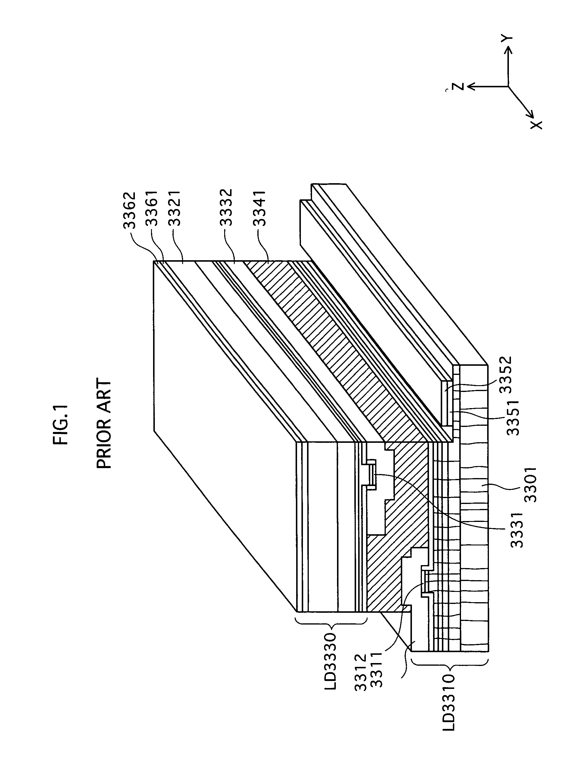
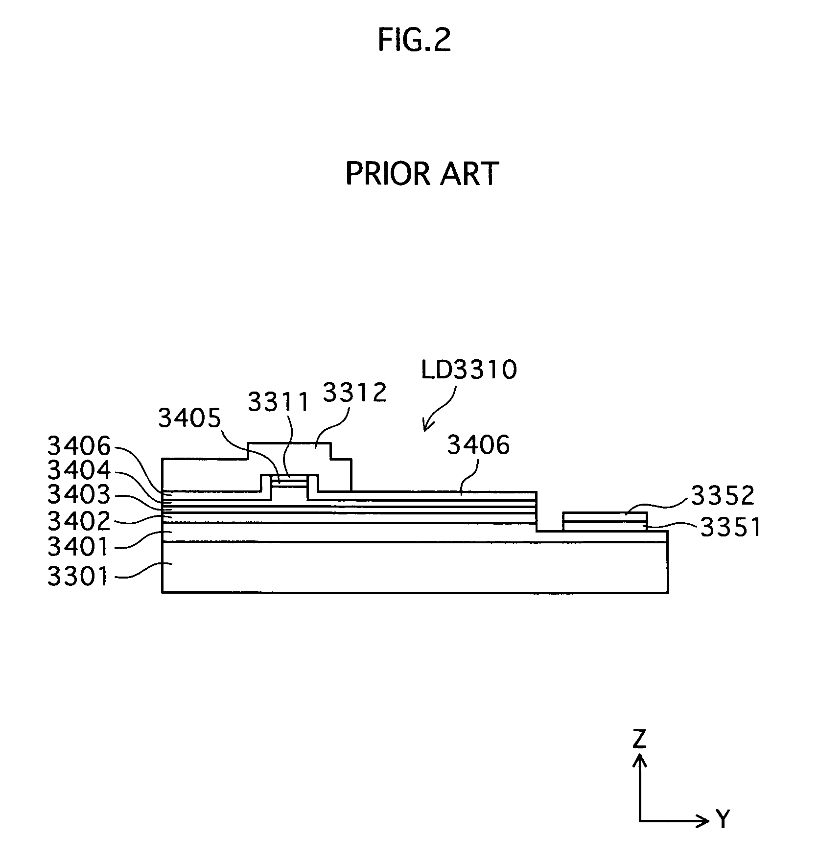
Integrated semiconductor laser diode module and manufacturing method of the same
a laser diode module and integrated technology, applied in the direction of semiconductor laser arrangement, semiconductor laser structure details, semiconductor lasers, etc., can solve the problems of increasing production costs, difficult to make the facets flat for both laser diodes with the conventional manufacturing method, and inability to obtain flat cleavage planes for both laser diodes, etc., to achieve a wide range of production yield and suppress damage to the wafers. , the effect of improving the yield
- Summary
- Abstract
- Description
- Claims
- Application Information
AI Technical Summary
Benefits of technology
Problems solved by technology
Method used
Image

Examples
first embodiment
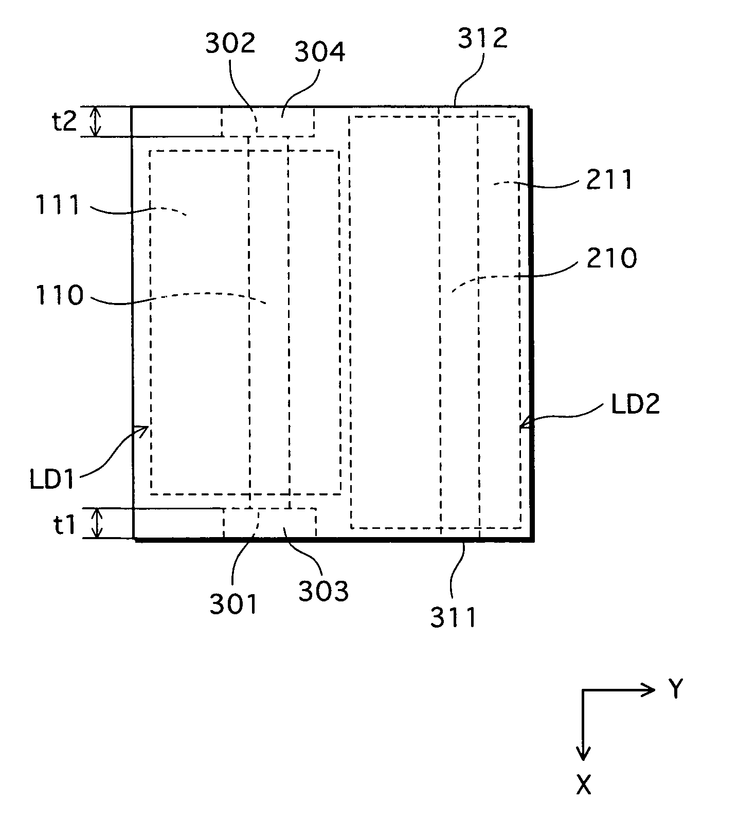
[0092]FIG. 10 is a schematic perspective view illustrating a structure of an integrated semiconductor laser diode module of a First Embodiment according to the present invention. FIG. 11 is a schematic sectional view of the integrated semiconductor laser diode module. The integrated semiconductor laser diode module is such that a 400 nm band laser diode LD 1 made of gallium nitride semiconductor and a 650 nm band laser diode LD 2 made of aluminum gallium indium phosphide semiconductor are joined together by a joining member 100 so as to be integrated.
[0093] The LD 1 has a structure described below. On an n-type GaN (0001) substrate 101 that is 70 μm thick, an undoped n-type layer 102 that is about 1 μm thick and made of Al0.01Ga0.99N is formed. On the n-type layer 102, an n-type clad layer 103 that is about 1 μm thick and made of Al0.07Ga0.93N is formed. On the n-type clad layer 103, an emission layer 104 is formed. The emission layer 104 includes a Multiple Quantum Well (MQW) acti...
second embodiment
[0132] The following explains a Second Embodiment with reference to FIGS. 31-36. In the Second Embodiment, the reflectance of the emitting facets, from which laser beams are emitted, of the LD 1 and LD 2 are separately optimized. FIG. 31 shows a step of forming a first coating film, after the steps shown by A-C in FIG. 19 of exposing the facets by making the opening 1000 to the LD 1. This drawing is a sectional view corresponding to C of FIG. 19.
[0133] After forming an emitting facet 2201 of the LD 1, a SiO2 mask 2202 for forming the facets is removed using the hydrofluoric acid etchant, for example (FIG. 32). Note that the emitting facet 2201 is just an example of “an emitting facet of a laser diode”. Further, as shown in FIG. 33, a first coating film 2401 is formed so as to be about 73 nm in thickness on the facets. The first coating film 2401 made of SiO2 film is then formed on an upper surface of the LD 1 wafer using the plasma CVD method, for example.
[0134] Next, as shown in ...
third embodiment
[0143] An example described by the above first and second embodiments, as shown in FIG. 28, is such that the back surfaces of the substrates of the LD 1 and LD 2 are polished to make the substrates thinner, the n-side ohmic electrode and n-side pad electrode are formed on the substrate, and then the LD 1 wafer and LD 2 wafer are joined together. However, in the third embodiment, first, the wafers are joined together, next, the substrates are made thinner by polishing, and then, the n-side ohmic electrode and n-side pad electrode are formed on the back surfaces of the substrates.
[0144]FIGS. 37-41 are schematic views to explain such steps.
[0145]FIG. 37 illustrates the LD 1 wafer before joining. The LD 1 wafer is manufactured in the same steps described in FIG. 17 of the present invention, and then completed by forming the p-side pad electrode 111 over the p-side ohmic electrode 110 so as to cover the opening of the dielectric layer 109.
[0146]FIG. 38 illustrates the LD 2 wafer befor...
PUM
 Abstract
Description
Claims
Application Information