Method of controlling the uniformity of PECVD-deposited thin films

a technology of pecvd and uniformity, applied in the direction of chemical vapor deposition coating, plasma technique, coating, etc., can solve the problem of non-uniform film thickness of precursor source gas, achieve better control over surface standing wave effect and film thickness uniformity, improve film thickness uniformity, and reduce the effect of film deposition ra

Inactive Publication Date: 2005-10-20
APPLIED MATERIALS INC
View PDF36 Cites 65 Cited by
  • Summary
  • Abstract
  • Description
  • Claims
  • Application Information

AI Technical Summary

Benefits of technology

[0032] An a-SiNx:H gate dielectric film exhibiting the physical characteristics listed above provides excellent performance capabilities, and the uniformity of the film across the substrate enables the production of flat panel displays having dimensions in the range of 1900 mm×2200 mm, and possibly even larger.
[0046] The width of the plasma sheath can be increased, for example (and not by way of limitation), by decreasing the spacing between the upper and lower electrodes in a parallel plate processing chamber.
[0048] As mentioned above, a reduction in the RF power to the plasma source to within the range of about 0.2 W / cm2 to about 0.6 W / cm2 can aid in improving film thickness uniformity. Although a decrease in RF power also decreases the film deposition rate, we have found, that for a silicon-containing PECVD deposited film, this range of RF power typically provides an acceptable film deposition rate of at least 1,000 Å / min, by way of example and not by way of limitation).
[0049] The PECVD process parameters described above, when used in combination, provide better control over surface standing wave effects and film thickness uniformity for silicon-containing films such as silicon nitride and silicon oxide. Our initial indications are that PECVD-deposited a-Silicon films are not as significantly affected by standing wave effects.

Problems solved by technology

However, we discovered that when the substrate size was increased to dimensions of 1500 mm to 1800 mm, this precursor source gas produced a non-uniform film thickness which varied by as much as about 25%; produced film structures where the Si—H bonded content exceeded 23 atomic %; and, produced films where the wet etch rate in HF solution (normalized to thermal oxide 1000 Å / min) exceeded 2400 Å / min in some instances.

Method used


Image

  • Method of controlling the uniformity of PECVD-deposited thin films
  • Method of controlling the uniformity of PECVD-deposited thin films
  • Method of controlling the uniformity of PECVD-deposited thin films

Examples


example one

PECVD Deposition of a-SiNx:H Gate Dielectric Layers by Increasing the Concentration of NH3 in the Precursor Gas Composition

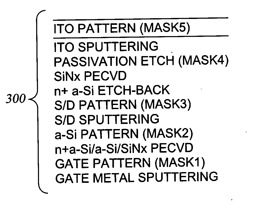
[0103] We have previously described all of the performance requirements for the a-SiNx:H gate dielectric layer. We carried out extensive experimentation in an effort to produce a PECVD deposited a-SiNx:H gate dielectric layer which met the performance requirements and which provided a uniformity in film thickness and uniformity in film properties, including structural and chemical composition, when PECVD deposited over a large surface area, larger than 1000 mm×1000 mm, for example. One basic requirement is that the a-SiNx:H film deposition rate is more than 1000 Å / min, and typically more than 1300 Å / min, so that the fabrication throughput for the TFT provides adequate productivity to be economically competitive. The basic requirements for the a-SiNx:H film are that: the Si—H bonded content of the a-SiNx:H film is less than about 15 atomic %; the film stress ran...

example two

PECVD Deposition of a-SiNx:H Gate Dielectric Layers of Uniform Thickness by Controlling a Combination of Process Parameters

[0122] As discussed above, we have discovered that controlling a combination of PECVD deposition process parameters during deposition of silicon-containing thin film provides improved control over surface standing wave effects. These process parameters include: the spacing between the upper and lower electrodes in the plasma reactor; the RF frequency of the plasma source; the RF power to the plasma source; the process chamber pressure; and the relative concentrations of the various components in the precursor gas composition.

[0123] We performed a series of experiments to determine the advantageous ranges for each process parameter, in order to provide maximum control over surface standing wave effects and uniformity of film properties (especially film thickness). A comparison between film uniformity available prior to the present invention and film uniformity ...


PUM

PropertyMeasurementUnit
equivalent radiusaaaaaaaaaa
pressureaaaaaaaaaa
pressureaaaaaaaaaa

Abstract

We have discovered that controlling a combination of PECVD deposition process parameters during deposition of silicon-containing thin film provides improved control over surface standing wave effects. By minimizing surface standing wave effects, the uniformity of film properties (particularly film thickness) across a substrate surface onto which the films have been deposited is improved. The process parameters which have the greatest effect on surface standing wave effects include: the spacing between the upper and lower electrodes in the plasma reactor; the RF frequency of the plasma source; the amount RF power to the plasma source; the process chamber pressure; the relative concentrations of the various components in the precursor gas composition; and the precursor gas overall flow rate relative to the substrate processing volume.

Description

RELATED APPLICATIONS [0001] This application is a continuation-in-part of U.S. application Ser. No. 10 / 829,016, filed Apr. 20, 2004, which is currently pending.BACKGROUND OF THE INVENTION [0002] 1. Field of the Invention [0003] The present invention pertains to a method of controlling surface standing wave effects during PECVD deposition of a silicon-containing thin film. By controlling surface standing wave effects during film deposition, the uniformity of a silicon nitride film deposited by PECVD (plasma-enhanced chemical vapor deposition) can be tightly controlled over a large surface area. [0004] 2. Brief Description of the Background Art [0005] Current interest in thin film transistor (TFT) arrays is particularly high because these devices are used in liquid crystal active matrix displays of the kind often employed for computer and television flat panels. The liquid crystal active matrix displays may also contain light emitting diodes for back lighting. Further, organic light e...

Claims


Application Information

Patent Timeline
Patent Type & Authority Applications(United States)
IPC IPC(8): C23C16/34H01L21/318
CPCH01L21/3185H01L21/02274H01L21/0214H01L21/02164H01L21/02211H01L21/0217
Inventor CHOI, SOO YOUNGWON, TAE KYUNGWHITE, JOHN M.
Owner APPLIED MATERIALS INC
Why Eureka
Try Eureka