Micro-structured gas sensor with control of gas sensitive properties by application of an electric field

a gas sensor and microstructure technology, applied in the field of gas sensors, can solve the problem that the design does not take into account the planar manufacturing method of conventional semiconductor fabrication, and achieve the effect of gaining selectivity

Inactive Publication Date: 2005-10-27
MICRONAS
View PDF4 Cites 25 Cited by
  • Summary
  • Abstract
  • Description
  • Claims
  • Application Information

AI Technical Summary

Benefits of technology

[0030] A kinetic effect can also be introduced by modulating the gate voltage. Operation with a time-varying gate voltage periodically shifts the Fermi level in the metal oxide, that is, alteration of the electrochemical equilibrium under the effect of an external voltage on the field electrode. Periodic modulation of the gate voltage leads to an alternating variation in the resistance of the sensitive film. Through spectral analysis of

Problems solved by technology

A disadvantage of known arrangements of these sensors is that no design takes into account the planar manufacturing methods of conventional semiconductor fabrication.
Because it requires very high electric fields

Method used


Image

  • Micro-structured gas sensor with control of gas sensitive properties by application of an electric field
  • Micro-structured gas sensor with control of gas sensitive properties by application of an electric field
  • Micro-structured gas sensor with control of gas sensitive properties by application of an electric field

Examples


Embodiment Construction

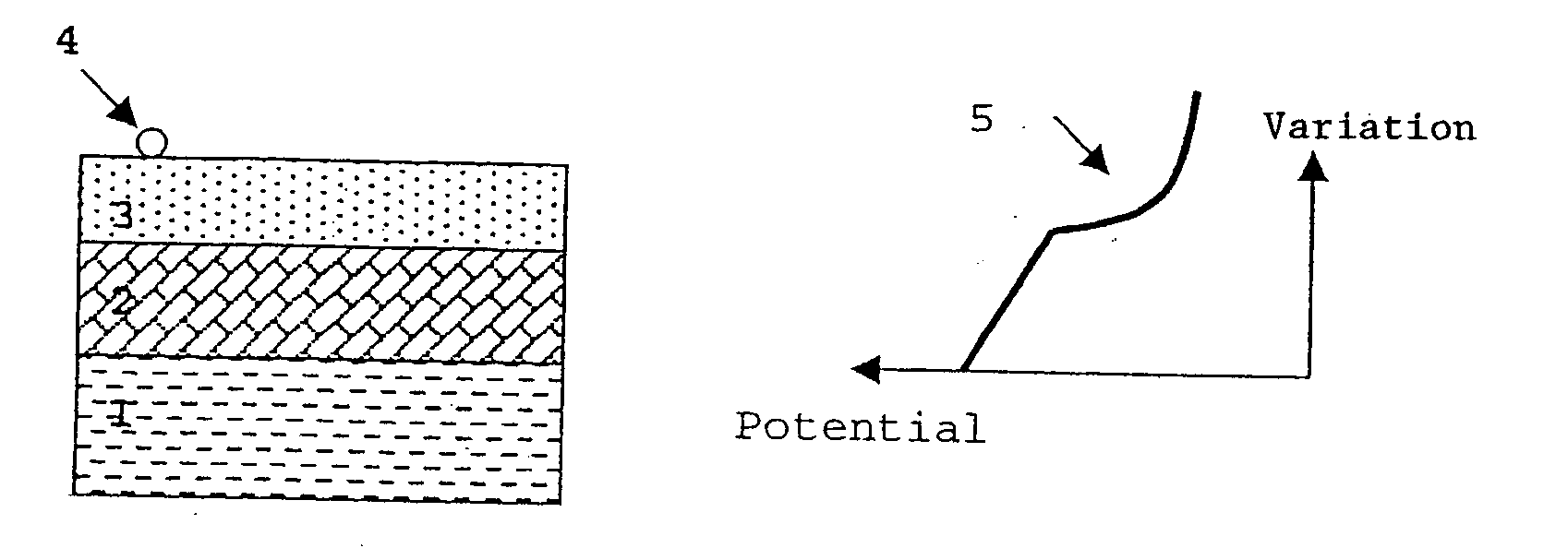
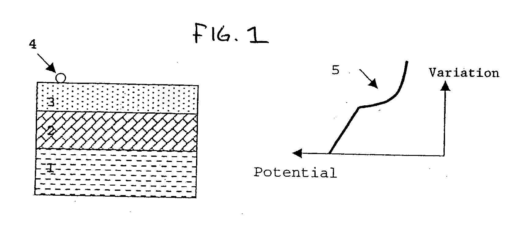
[0041] Referring to FIG. 1, a gas sensor includes an electrode 1 disposed under a gas-sensitive semiconductor film 3 with an insulator layer 2 in between. The aforementioned electroadsorptive effect may occur when the thickness of the gas-sensitive semiconductor film 3 is on the order of the Debye length LD. In this way the surface absorption of gas molecules 4 can be controlled through an electric field. Further, the insulator layer 2 may be low in defects because these defects can substantially shorten the Debye length of the insulator layer 2 and thus interfere with penetration of the field to the gas-sensitive film 3. Examples of Debye lengths for SnO2 are 60-80 nm where for insulators these lengths may be in the range below several micrometers.

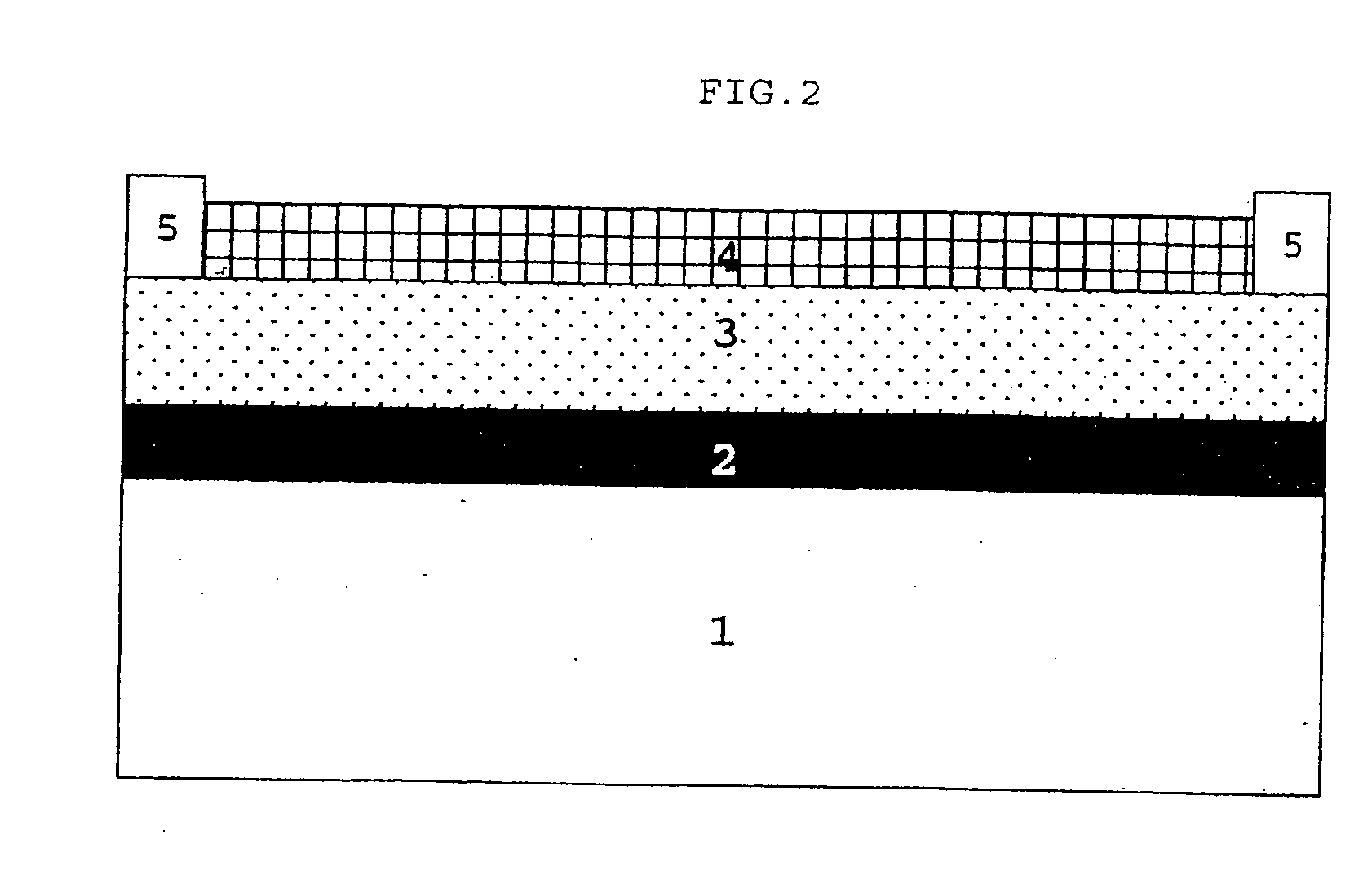
[0042] Referring to FIG. 2, the gas sensor includes a semiconductor substrate 1 on which is disposed a gas-sensitive film 4 with a thickness of for example 59 nm. The gas-sensitive film 4 may be contacted by two electrodes 5. The gas-sen...


PUM


Abstract

A gas sensor includes a semiconductor substrate on which is disposed at least one field electrode, and advantageously a plurality of field electrodes. The field electrodes are disposed under a gas-sensitive semiconductor resistive film, with an insulator layer in between. The film, which may be in electrical contact with a pair of external electrodes, may comprise a metal oxide, such as for example SnO2, WO3, In2O3, Ga2O3, Cr2-xTixO3+z, or various organic semiconductors. The field electrodes produce an electric field acting on the semiconductor, and an electroadsorptive effect may occur when the thickness of the gas-sensitive film is on the order of the Debye length. In the case of the known gas-sensitive material SnO2, for example, the Debye length may be approximately 60 to 80 nm. An electric field produced in the body of the gas sensor may be effective up to the surface of the gas-sensitive film that is exposed to the gas, i.e., the films lying above the gate electrode do not screen the electric field. The use of a plurality of field electrodes may make it possible to offset or control the gradient in the surface potential variation.

Description

PRIORITY INFORMATION [0001] This application claims priority from German application 102 10 819.6, filed Mar. 12, 2002 and International application PCT / EP03 / 02544 filed Mar. 12, 2003. BACKGROUND OF THE INVENTION [0002] The invention relates in general to gas sensors and in particular to a microstructured gas sensor having gas sensitive properties that are controlled by application of an electric field. [0003] Microstructured gas sensors are disclosed for example in German published patent applications DE 44 42 396 A1 and DE 195 44 303 A1. In recent years, resistance-type gas sensors have been increasingly used to measure air pollutant concentrations in the ppm and ppb ranges. Advantages of such semiconductor gas sensors include relatively low manufacturing cost along with the simplicity of hybrid integration into electronics for the conditioning of the measured signals. Semiconductor gas sensors are typically electrical conductance or resistance sensors. At operating temperatures o...

Claims


Application Information

Patent Timeline
IPC IPC(8): G01N27/12G01N33/00
CPCG01N27/128G01N27/123G01N27/12G01N27/416
Inventor DOLL, THEODORBOTNER, HARALDWOLLENSTEIN, JURGENJAGLE, MARTINLEHMANN, MIRKO
Owner MICRONAS
Why Eureka
Try Eureka