Optical devices featuring textured semiconductor layers

a technology of optical devices and semiconductor layers, applied in the direction of semiconductor devices, electrical devices, nanotechnology, etc., can solve the problems of reduced internal efficiency and achieve the effects of enhancing light escape, improving light extraction efficiency, and improving the efficiency of coupling light into the devi

Inactive Publication Date: 2005-11-03
TRUSTEES OF BOSTON UNIV
View PDF57 Cites 94 Cited by
  • Summary
  • Abstract
  • Description
  • Claims
  • Application Information

AI Technical Summary

Benefits of technology

[0005] The present invention provides a device for use as a light emitter or sensor or as a solar cell. For an emitter of the invention, the IQE and light extraction efficiency is improved over conventional devices. For a sensor or solar cell, the efficiency of coupling light into the device is also improved. In one embodiment, the semiconductor material is deposited in layers, starting with as grown textured initial semiconductor layer deposited onto a substrate. In one embodiment, the layer is textured as grown on the substrate so as to have a textured surface morphology. The substrate and textured layer can be used as a template for the growth of multiple semiconductor layers. For example, a device may comprise a second layer deposited onto the first textured layer. These layers can be deposited with p and n dopants to form a p-n junction light emitting diode (LED). The textured emitting layer enhances light escape. The initial semiconductor layer preferably serves as a barrier layer onto which a quantum well layer is grown. Each of the semiconductor layers conforms to the texture of the first grown layer and thus the external surface of the LED from where the light is extracted has approximately the same texture as the initial semiconductor layer.
[0006] Preferably, multiple quantum wells comprising a plurality of barrier and quantum well layers are deposited on one another as alternating semiconductor layers each replicating the original texture. The texturing replicated through the barrier and well layers repositions the quantum wells so that their surfaces are not perpendicular to the [0001] polar direction and thus the quantum wells maintain their square well shape since they are not distorted by internal fields due to polarization. As a result the hole and electron wavefunctions overlap leading to efficient recombination and thus drastically improving the IQE.

Problems solved by technology

In the case of Nitride LEDs grown along polar (0001) and (000-1) directions the internal efficiency is also reduced due to the distortion of the quantum wells between the n- and p-doped layers caused by the internal electric fields.

Method used


Image

  • Optical devices featuring textured semiconductor layers
  • Optical devices featuring textured semiconductor layers
  • Optical devices featuring textured semiconductor layers

Examples


example i

[0054] A textured GaN template according to the invention is grown by the modified HVPE process described above. The GaN template is grown via a modified HVPE reactor. In the reactor, a group III precursor is GaCl gas, which can be synthesized upstream by flowing HCl on a quartz-boat containing Ga at temperatures from about 500° C. to 1000° C. GaCl gas then mixes with ammonia (NH3) downstream near the surface of the substrate wafer to form GaN at temperatures between about 900° C. to 1200° C. A GaN or AlN or AlGaN template of the invention can be grown along polar and non-polar directions. The templates can also grow in their cubic structure by choosing a substrate having cubic symmetry such as for example (100)Si (001)GaAs. In this case the subsequent nitride layers grown on it will have cubic symmetry as well.

[0055] The modified reactor is generally divided into four zones in which each zone temperature can be individually controlled. The reactor also has three separate delivery ...

example ii

[0062] Example II involves the growth of multiple (wrinkled) quantum wells on a textured template of the invention. The quantum wells comprise ten pairs of AlGaN and GaN layers. An individual GaN layer may comprise a textured quantum well layer with the AlGaN layer serving as the barrier layer. The composition of the AlGaN layer, for example, is Al0.2Ga0.8N. Generally, that is AlxGa1-xN. The multiple quantum wells can also be made by any combination of small gap III-V nitride films (wells) and large gap III-V nitride films (barriers). The composition of the MQW determines the emission energy of light from about 0.7 eV of pure InN to 6 eV from pure AlN. The plurality of quantum well layers are grown by any suitable deposition process. A MBE process involves the reaction of a group III material with nitrogen that has been activated by radio frequency or microwave plasma. An alternative approach would be to react group III materials with ammonia on a heated substrate.

[0063] The group ...

example iii

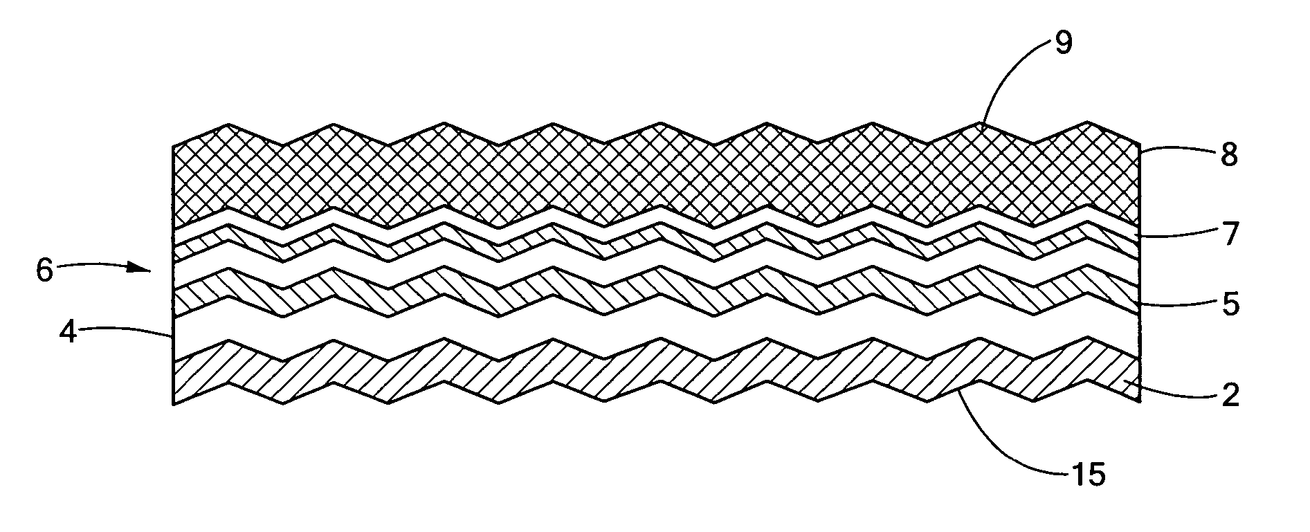
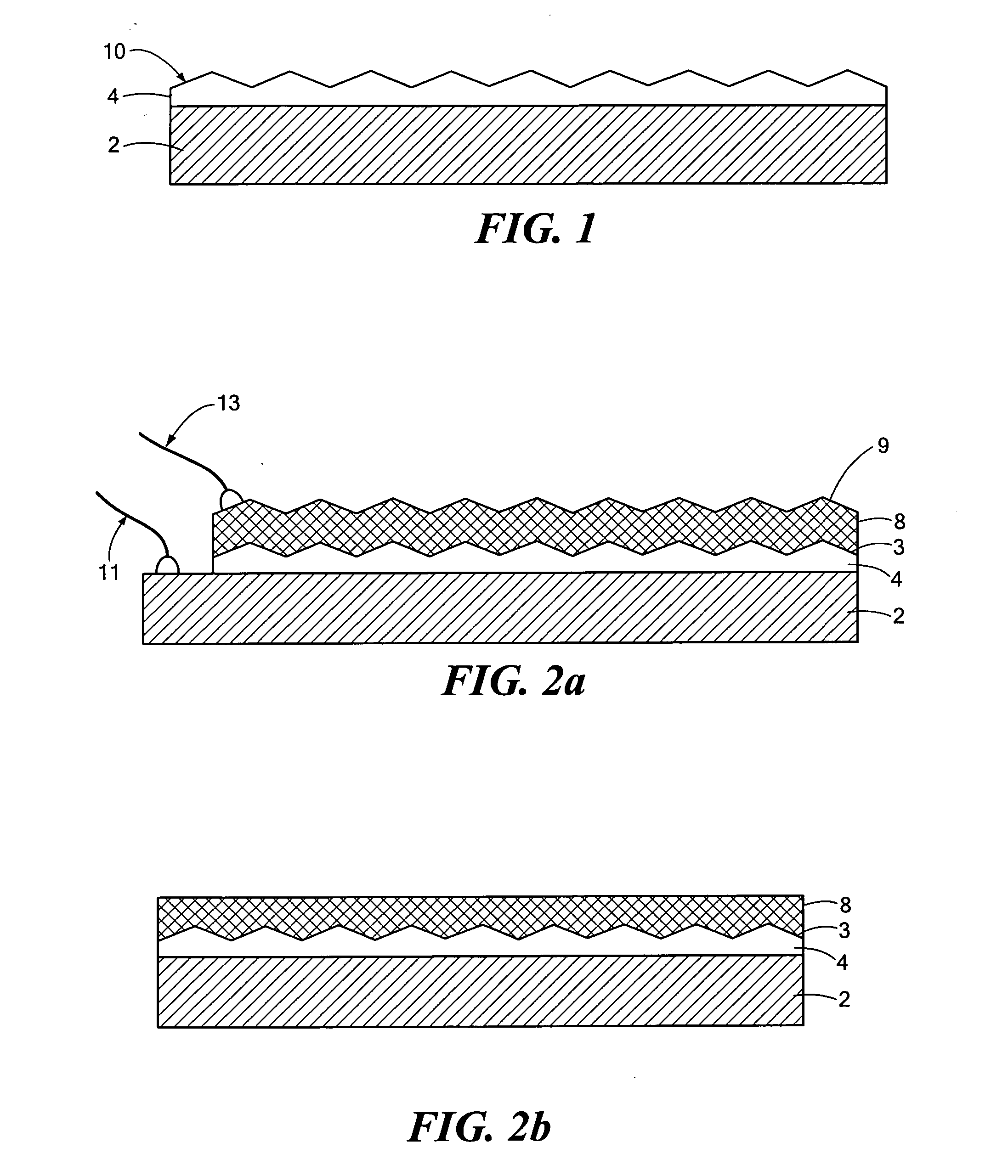
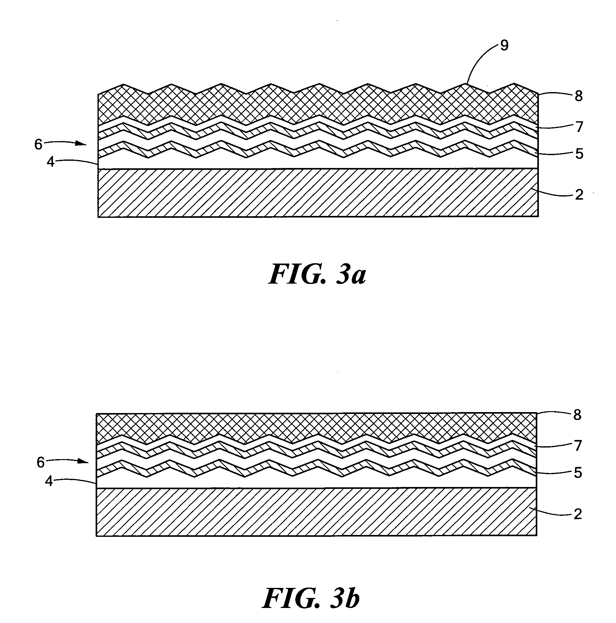
[0069] A highly conductive magnesium-doped p-type GaN layer with a hole concentration of about 1018 cm−3 and a thickness of about 0.5 micrometers was deposited by molecular beam epitaxy (MBE) on top of an n-type textured gallium nitride template according to the invention. The textured gallium nitride template had an electron concentration of about 1019 cm−3. The p-type GaN layer was formed using a radio frequency plasma source to activate molecular nitrogen and Knudsen effusion cells to evaporate the Ga and Mg. Growth occurred at extreme gallium rich conditions at which Mg was then incorporated at relatively high substrate temperatures of 700° C. to 800° C. Alternatively, the p-type layer could be grown using ammonia as the nitrogen source. A similar p-type layer could also have been grown by an MOCVD or HVPE process. FIG. 12 shows an electroluminescence spectrum of the p-n junction formed with the textured template under a current injunction of 80 mA.


PUM


Abstract

A semiconductor sensor, solar cell or emitter or a precursor therefore having a substrate and textured semiconductor layer deposited onto the substrate. The layer can be textured as grown on the substrate or textured by replicating a textured substrate surface. The substrate or first layer is then a template for growing and texturing other semiconductor layers from the device. The textured layers are replicated to the surface from the substrate to enhance light extraction or light absorption. Multiple quantum wells, comprising several barrier and quantum well layers, are deposited as alternating textured layers. The texturing in the region of the quantum well layers greatly enhances internal quantum efficiency if the semiconductor is polar and the quantum wells are grown along the polar direction. This is the case in nitride semiconductors grown along the polar [0001] or [000-1] directions.

Description

CROSS REFERENCE TO RELATED APPLICATIONS [0001] This application claims the priority of U.S. Provisional Application No. 60 / 562,489 filed Apr. 15, 2004 and entitled, FORMATION OF TEXTURED III-NITRIDE TEMPLATES FOR THE FABRICATION OF EFFICIENT OPTICAL DEVICES, U.S. Provisional Application No. 60 / 615,047 filed Oct. 1, 2004 and entitled, FORMATION OF TEXTURED III-NITRIDE TEMPLATES FOR THE FABRICATION OF EFFICIENT OPTICAL DEVICES, and U.S. Provisional Application No. 60 / 645,704 filed Jan. 21, 2005 and entitled, NITRIDE LEDS BASED ON FLAT AND WRINKLED QUANTUM WELLS, which are each hereby incorporated by reference herein.STATEMENT REGARDING FEDERALLY SPONSORED RESEARCH OR DEVELOPMENT [0002] Part of the work leading to this invention was carried out with United States Government support provided under Contract No. DAAD19-00-2-0004 awarded by United States Army Research Office. Thus, the United States Government has certain rights in this invention.BACKGROUND OF THE INVENTION [0003] A light ...

Claims


Application Information

Patent Timeline
Patent Type & Authority Applications(United States)
IPC IPC(8): H01L29/15H01L29/20H01L29/24H01L31/0236H01L31/0352H01L31/18H01L33/22H01L33/24H01L33/32
CPCB82Y20/00H01L29/155H01L29/2003H01L31/0236H01L31/035236H01L31/035281Y02E10/544H01L31/184H01L31/1852H01L33/22H01L33/24H01L33/32H01L31/03529H01L31/02363H01L31/02366
Inventor MOUSTAKAS, THEODORE D.CABALU, JASPER S.
Owner TRUSTEES OF BOSTON UNIV
Why Eureka
Try Eureka