Method for forming a photonic band-gap structure and a device fabricated in accordance with such a method

a technology of photonic band gap and fabricated device, which is applied in the direction of waveguide type devices, instruments, optical elements, etc., can solve the problems of incompatible silicon-based technology, large structure size, and high cost of conventional methods for producing such a resonator, so as to achieve simple and cost-effective production and reduce the dimension

Active Publication Date: 2005-11-10
ATMEL CORP
View PDF6 Cites 3 Cited by
  • Summary
  • Abstract
  • Description
  • Claims
  • Application Information

AI Technical Summary

Benefits of technology

[0013] It is therefore an object of the present invention to provide a fabrication method for a PBG structure and a device having a PBG structure fabricated in accordance with such method, whereby the PBG structure and a reliable device both for filter and for micro-cavity applications can be produced simply and cost-effectively, whereby smaller dimensions are thus realized.

Problems solved by technology

A defect such as this creates a narrow pass-band frequency range within the larger stop-band frequencies.
Conventional methods for producing such a resonator are costly and the components of the resulting structures are big in size and are not compatible with silicon-based technologies for the fabrication of integrated semiconductor circuits.
The disadvantage of this approach, however, has proven to be the fact that with these methods, components are constructed that can only be used in filter applications and not, for example, in micro-cavity applications for resonators.
Furthermore, the structure of devices such as these requires several periods of artificial cells of electromagnetic crystals equal to half the wavelength of the signal.
This results in big dimensions of the produced devices.

Method used


Image

  • Method for forming a photonic band-gap structure and a device fabricated in accordance with such a method
  • Method for forming a photonic band-gap structure and a device fabricated in accordance with such a method
  • Method for forming a photonic band-gap structure and a device fabricated in accordance with such a method

Examples


Embodiment Construction

[0034] Identical reference numerals in the figures designate substantially identical components, or components with substantially identical functions, unless indicated otherwise.

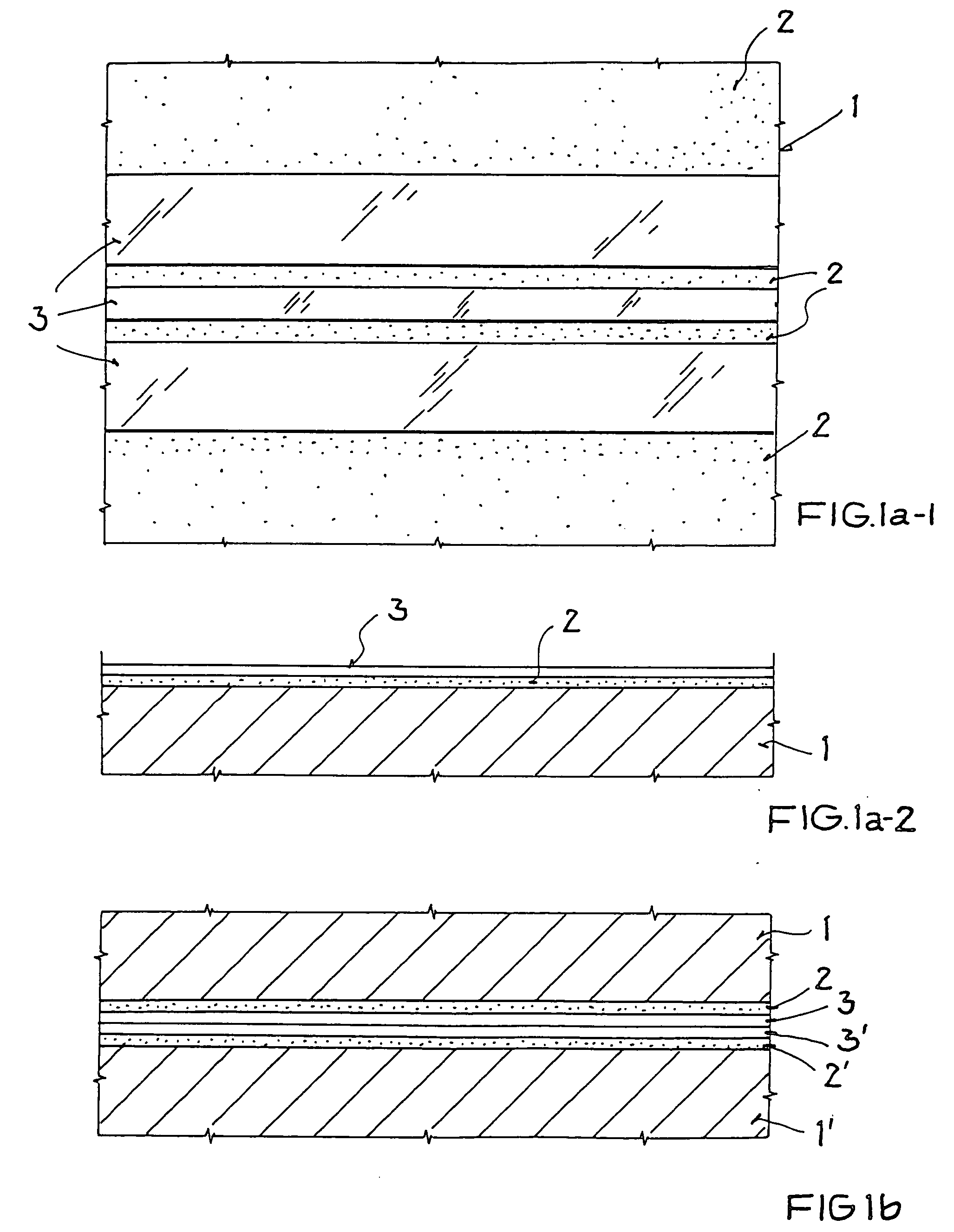
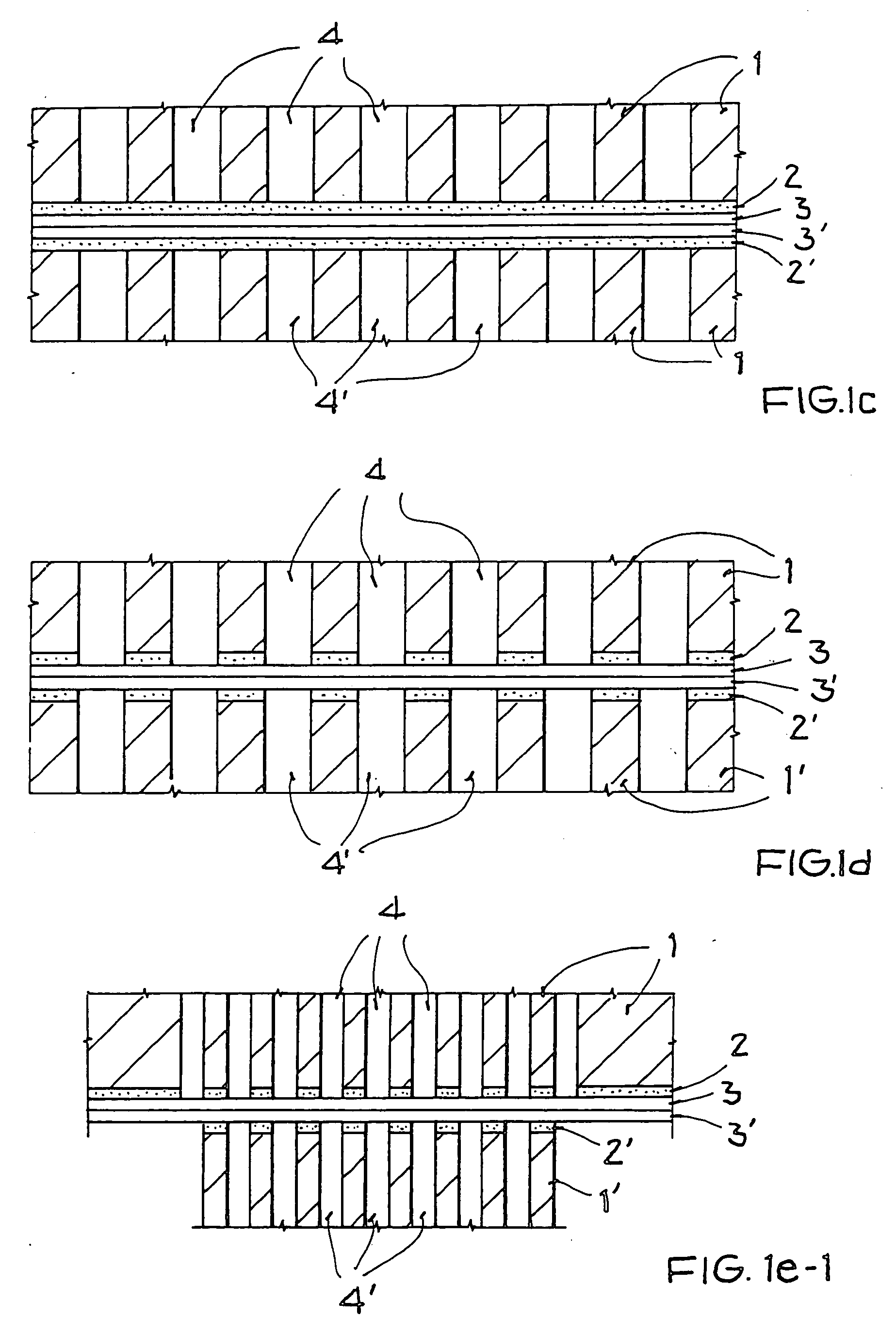
[0035] With reference to FIGS. 1a-1 to 1e-2, the individual method steps for producing a PBG structure in accordance with an example embodiment of the present invention are described in detail.

[0036]FIG. 1a-1 illustrates a top view and FIG. 1a-2 is a cross-sectional view of a substrate 1, on which a barrier layer, for example, a dielectric insulating layer 2, is formed. The dielectric insulating layer 2 can be, for example, 300 nm thick and can be made of silicon nitride or silicon dioxide. It will be obvious to one skilled in the art that other dielectric insulation materials can also be used. Furthermore, it is also noted that, the barrier layer 2 can also be omitted.

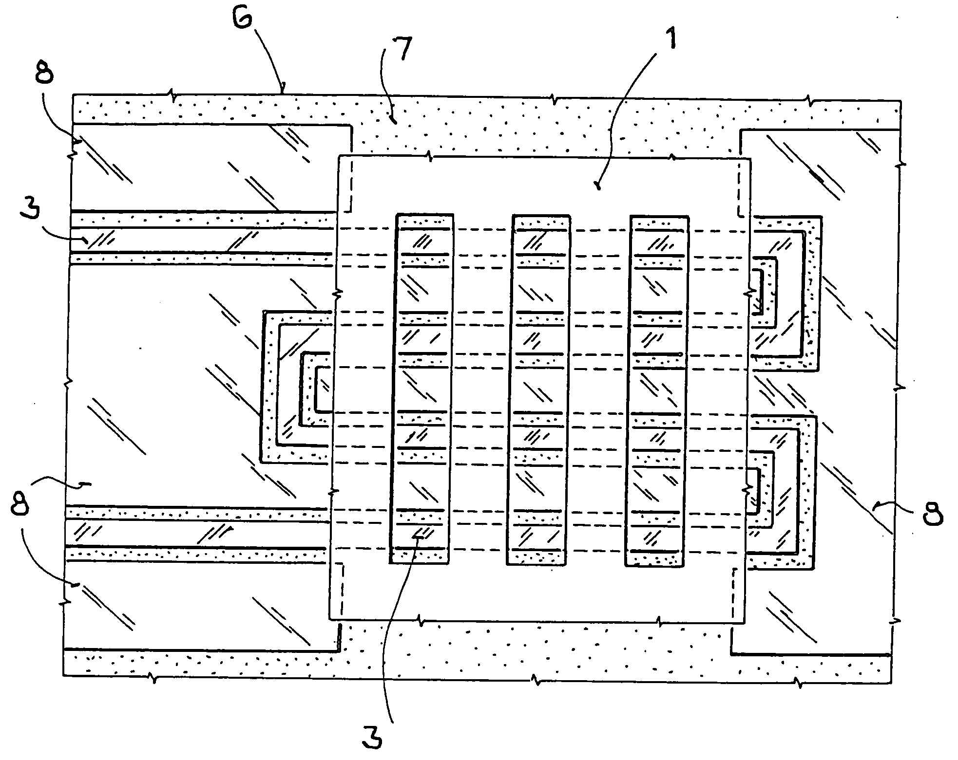
[0037] In a subsequent step, a structured coplanar waveguide metallization 3 is formed over the dielectric insulating layer 2 using, for e...


PUM

PropertyMeasurementUnit
thickaaaaaaaaaa
aspect ratioaaaaaaaaaa
resonance frequencyaaaaaaaaaa

Abstract

A device for application in the high frequency field and a method for forming a photonic band-gap structure are provided. The device being mountable on a primary substrate for forming the device. The device being formed by forming conformal coplanar waveguide metallizations on surface areas of two substrates, connecting the conformal coplanar waveguide metallizations of the two substrates, and structured back-etching of the two substrates, starting at surface areas of the two substrates that are opposite the coplanar waveguide metallizations.

Description

[0001] This nonprovisional application claims priority under 35 U.S.C. § 119(a) on German Patent Application No. DE 102004022140.5, which was filed in Germany on May 5, 2004, and which is herein incorporated by reference. BACKGROUND OF THE INVENTION [0002] 1. Field of the Invention [0003] The present invention relates to a method for forming a photonic band-gap structure (PBG structure) on a substrate and a device having a photonic band-gap structure that is fabricated according to such a method for application in, for example, microwave and / or millimeter wave technology, that is, in the high frequency field. [0004] Although applicable to any passive device, the present invention and the problems it is based on are described hereinbelow in regard to microwave and millimeter wave filters and electromagnetic hollow cavities, that is, micro cavities. [0005] 2. Description of the Background Art [0006] There is generally much interest in transmitting and guiding electromagnetic waves for...

Claims


Application Information

Patent Timeline
Patent Type & Authority Applications(United States)
IPC IPC(8): H01P1/201
CPCH01P1/2005Y10T29/49016Y10T29/49018H01P1/2013
Inventor JOODAKI, MOJTABA
Owner ATMEL CORP
Why Eureka
Try Eureka