

Plasma device
a technology of plasma and plasma gel, which is applied in the direction of chemical vapor deposition coating, manufacturing tools, coatings, etc., can solve the problems of reducing the etching rate, large amount of gas cannot flow, and degenerating etching shapes
- Summary
- Abstract
- Description
- Claims
- Application Information
AI Technical Summary
Benefits of technology
Problems solved by technology
Method used
Image

Examples
embodiment 1
[0351] (Embodiment 1)
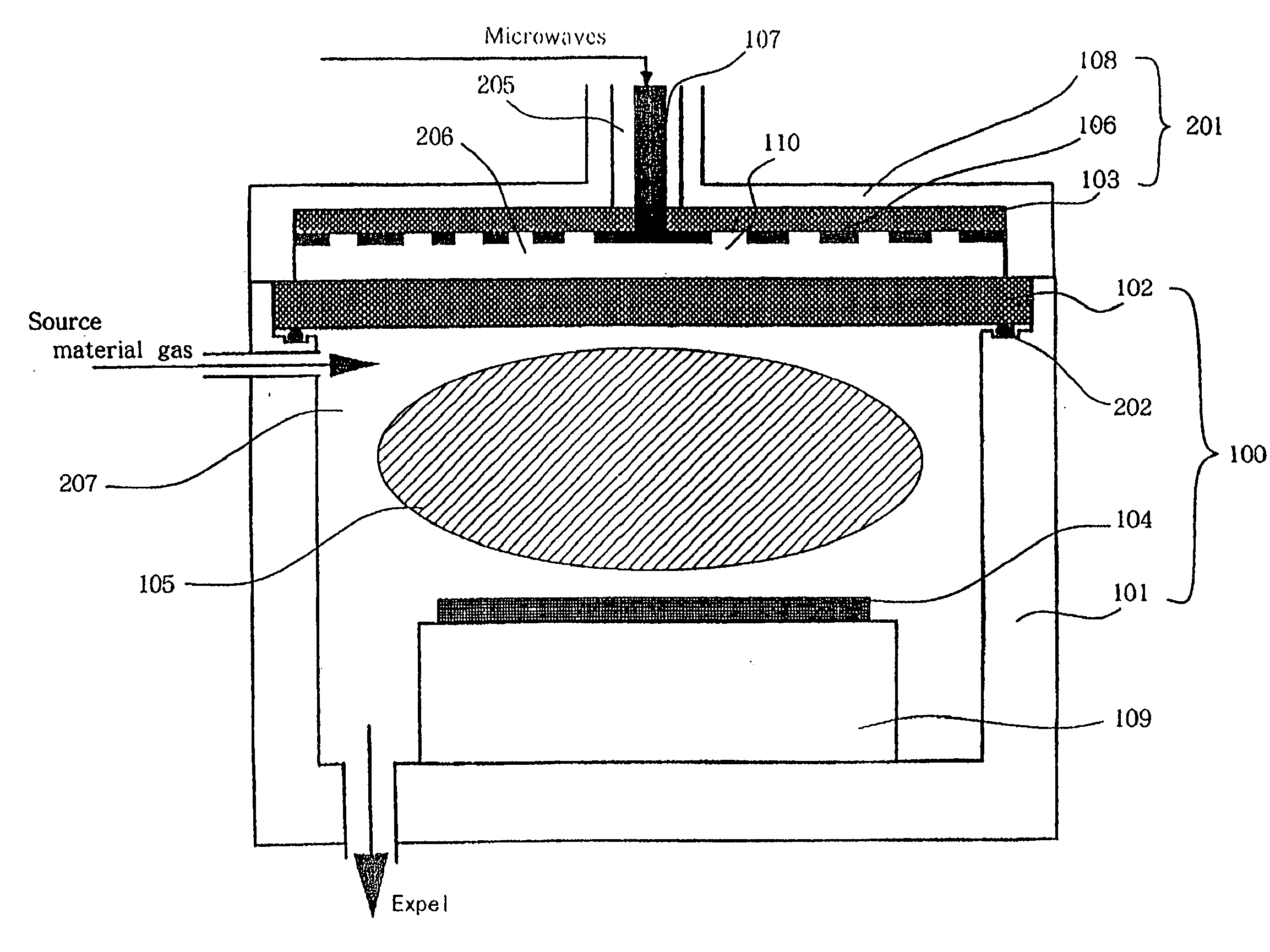
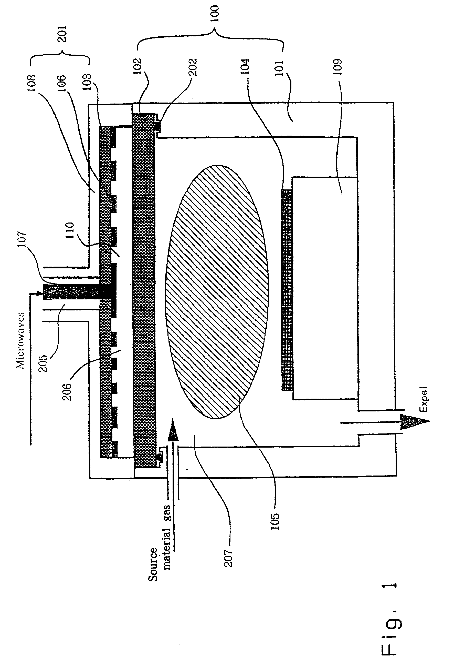
[0352] In this embodiment, when plasma is generated by introducing microwaves into a container using the plasma device shown in FIG. 1, the plasma stability is examined by varying the material of a member constituting an inner surface of the container, and the width of the member.
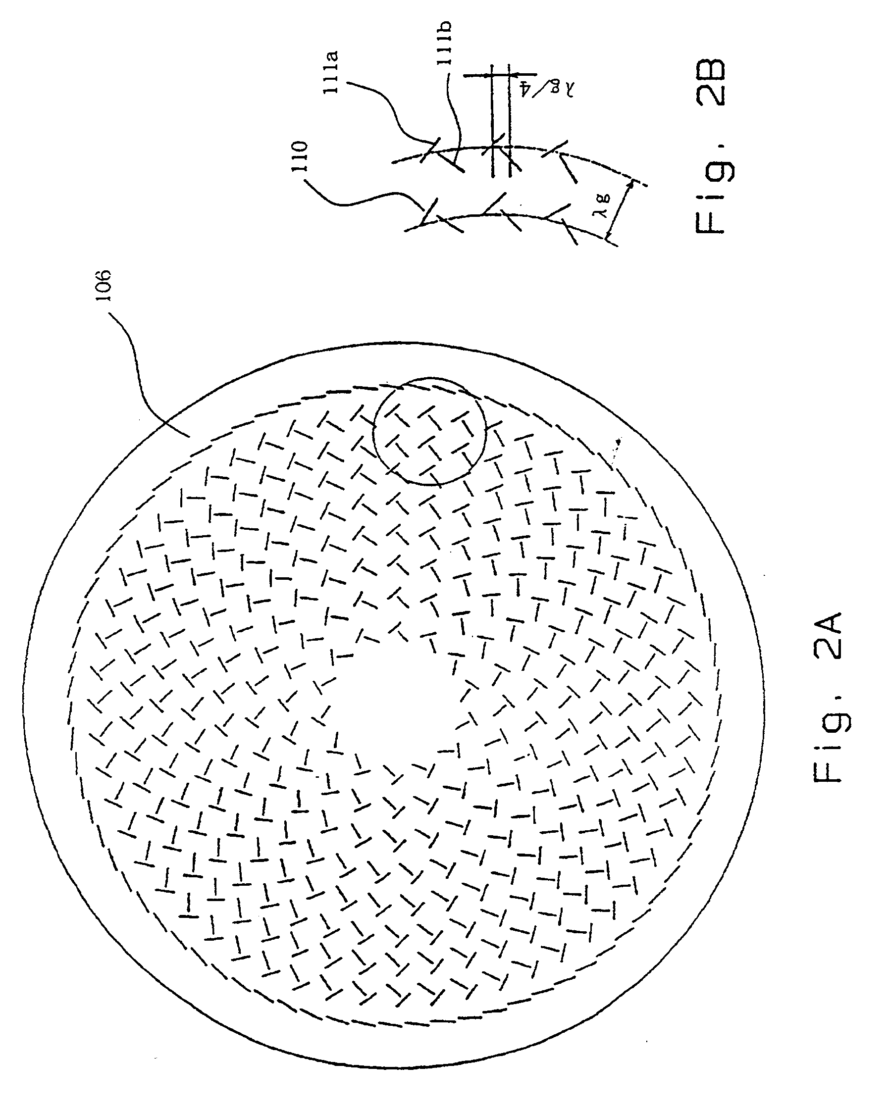
[0353] In FIG. 1, reference numeral 100 is a container capable of having its internal pressure reduced, reference numeral 101 is a chamber, reference numeral 102 is a first dielectric plate, reference numeral 103 is a waveguide dielectric plate, reference numeral 104 is an object to be treated, reference numeral 105 is plasma, reference numeral 106 is an antenna slot plate, reference numeral 107 is a coaxial tube, reference numeral 108 is an antenna guide, reference numeral 109 is an electrode, reference numeral 110 is a slot, reference numeral 201 is a radial line slot antenna, reference numeral 202 is a first O ring, reference numeral 205 is a space 3, reference numeral 206 is a spac...
embodiment 2
[0372] (Embodiment 2)
[0373] In this embodiment, the device of FIG. 5 is different from embodiment 1 in that a metallic thin film 114 is provided at a vacuum seal region where the first dielectric plate 102 (material: quartz) contacts a first O ring 202, as shown in FIG. 7, and the first O ring is not exposed to electromagnetic waves radiated from the antenna slot plate 106. Fluorine type resin is used as the material for the first O ring.
[0374]FIG. 8 is an enlarged view of region A in FIG. 7, and shows the case where the metallic thin film 114 is provided at a vacuum seal region where the first dielectric plate 102 (material: quartz) contacts a first O ring 202.
[0375] When the first O ring is made of a material such as resin that absorbs microwaves, it is directly heated by electromagnetic waves radiated from the antenna slot plate 106m as a result of discharge over a long time and it will be understood that damage will occur.
[0376] Therefore, metallic thin films each having a th...
embodiment 3
[0379] (Embodiment 3)
[0380] In this embodiment, as shown in FIG. 10, a device provided with a second dielectric plate 116, having a gas inlet 117 for supplying desired gas in a substantially uniform manner provided between the first dielectric plate 102 and the electrode 109 for holding the object to be treated 104, was used, and the uniformity of plasma 105 generated in the space 2 (109) was examined.
[0381]FIG. 10 shows the device incorporating the results of the second embodiment, and aluminum (Al) was coated to a thickness of 10 μm as a metallic thin film 114, at a region for vacuum sealing where the first dielectric plate 102 comes into contact with the first O ring 202. AlN (aluminum nitride) was used as the second dielectric plate 116 shown in FIG. 10. Since aluminum nitride contains nitrogen, it is characterized by the fact that there is less discharge gas compared to quartz.
[0382] In the device of FIG. 10, Ar gas was introduced into space 1 (208) as a plasma gas, and unifo...
PUM
| Property | Measurement | Unit |
|---|---|---|
| electron density | aaaaa | aaaaa |
| thickness | aaaaa | aaaaa |
| specific conductivity | aaaaa | aaaaa |
Abstract
Description
Claims
Application Information