Electron beam apparatus

a technology of electron beam and beam tube, which is applied in the direction of material analysis using wave/particle radiation, instruments, nuclear engineering, etc., can solve the problems of increased color aberration, image is more susceptible to blur, and cannot achieve the desired throughput of testing, so as to prolong the life and improve the luminance

Active Publication Date: 2005-11-17
EBARA CORP
View PDF7 Cites 33 Cited by
  • Summary
  • Abstract
  • Description
  • Claims
  • Application Information

AI Technical Summary

Benefits of technology

[0031] (11) The electron gun can emit beams at improved luminance and extend the lifetim

Problems solved by technology

When reflected electrons, rather than secondary electrons, are detected by a projection imaging electron beam apparatus, a test cannot be conducted at a desired throughput in some cases because a number of reflected electrons emitted from the surface of a sample is approximately 1/100 that of secondary electrons.
In some prior art examples, an ExB deflector is used to separate a primary electron beam from emitted electrons (secondary electrons or reflected electrons), but the use of the ExB deflec

Method used


Image

  • Electron beam apparatus
  • Electron beam apparatus
  • Electron beam apparatus

Examples


example

[0241] Indicated Direction: Right . . . Stage Moving Direction: Left (an image moves to the left=the field of view moves to the right)

[0242] Indicated Direction: Upward . . . Stage Moving Direction: Downward (an image moves downward=the field of view moves upward)

(2) Direct Entry of Coordinates on GUI:

[0243] Coordinates directly entered on the GUI are regarded as a location at which the operator wishes to view on the wafer coordinate system, so that the stage is moved such that the coordinate on a wafer are displayed at the center of a captured image.

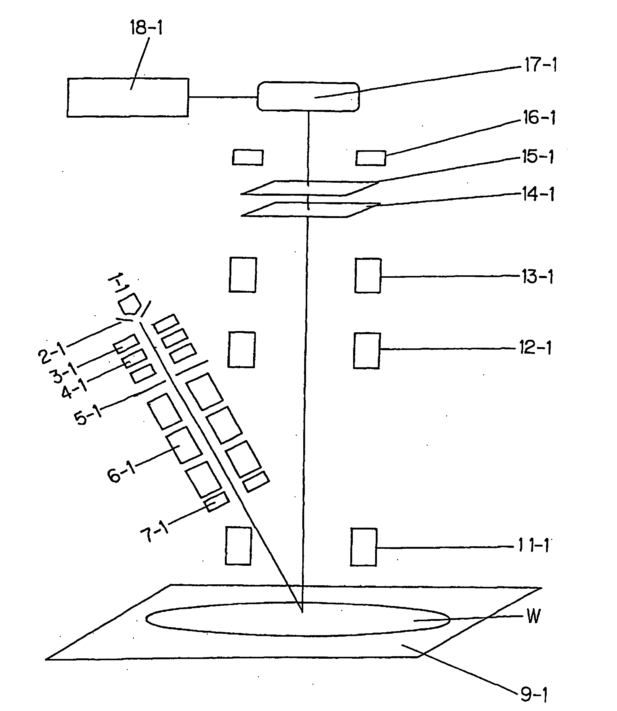
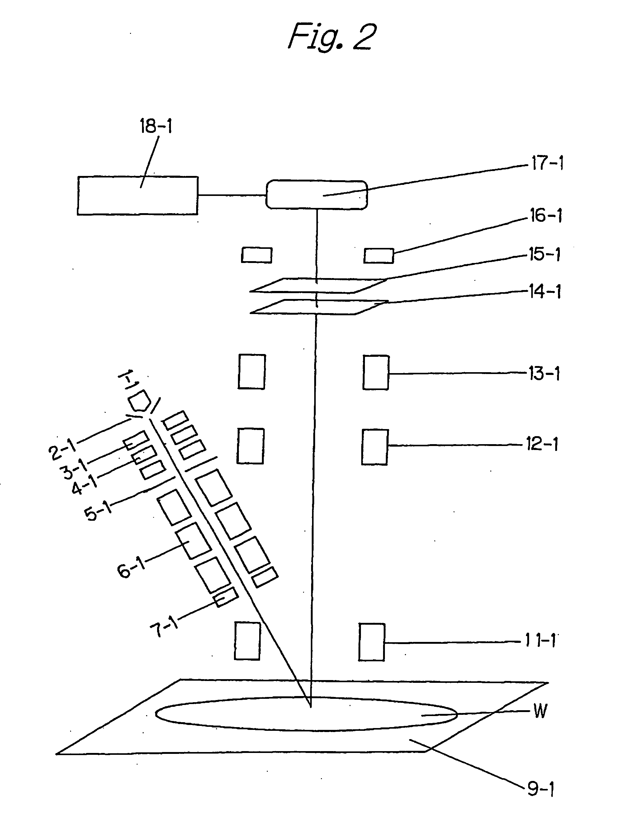
[0244] In the apparatus described in connection with FIG. 20, a procedure is taken to mount a correction ring on the electrostatic chuck, and position a wafer such that the wafer fits in the inner diameter of the correction ring. Therefore, in the inspection apparatus illustrated in FIG. 21, a procedure is taken to mount a correction ring on a wafer in the load lock chamber 22-1, integrally transfer the wafer mounted with the corre...


PUM


Abstract

An electron beam apparatus is provided for evaluating a sample at a high throughput and a high S/N ratio. As an electron beam emitted from an electron gun is irradiated to a sample placed on an X-Y-θ stage through an electrostatic lens, an objective lens and the like, secondary electrons or reflected electrons are emitted from the sample. The primary electron beam is incident at an incident angle set at approximately 35° or more by controlling a deflector. Electrons emitted from the sample is guided in the vertical direction, and focused on a detector. The detector is made up of an MCP, a fluorescent plate, a relay lens, and a TDI (or CCD). An electric signal from the TDI is supplied to a personal computer for image processing to generate a two-dimensional image of the sample.

Description

BACKGROUND OF THE INVENTION [0001] The present invention relates to an electron beam apparatus for testing (or inspecting), observing, and evaluating the surface of a sample such as a semiconductor wafer for structure, electric conduction and the like, and more particularly, to an electron beam apparatus which can accurately and reliably evaluate a pattern formed on a sample with a minimum line width of 0.15 μm or less at a high throughput. [0002] Conventionally, electron beam apparatuses have been known to irradiate an electron beam onto the surface of a semiconductor wafer, which is a sample under testing, for scanning to detect secondary electrons emitted from the wafer, generate image data of the surface of the wafer from captured signals indicative of the detected secondary electrons, and detect whether the image data matches or does not match each of dies on the wafer to detect defects on the wafer. [0003] Such an electron beam apparatus also includes a projection imaging elec...

Claims


Application Information

Patent Timeline
IPC IPC(8): G01N23/225H01J37/28
CPCG01N23/225H01J2237/24435H01J37/28
Inventor WATANABE, KENJISATAKE, TOHRUNAKASUJI, MAMORUMURAKAMI, TAKESHIKARIMATA, TSUTOMUNOJI, NOBUHARUTOHYAMA, KEIICHIHATAKEYAMA, MASAHIRO
Owner EBARA CORP
Why Eureka
Try Eureka