
Apparatus and method for multiple-gate semiconductor device with angled sidewalls

Active Publication Date: 2005-11-17
TAIWAN SEMICON MFG CO LTD
View PDF3 Cites 32 Cited by
  • Summary
  • Abstract
  • Description
  • Claims
  • Application Information

AI Technical Summary

Benefits of technology

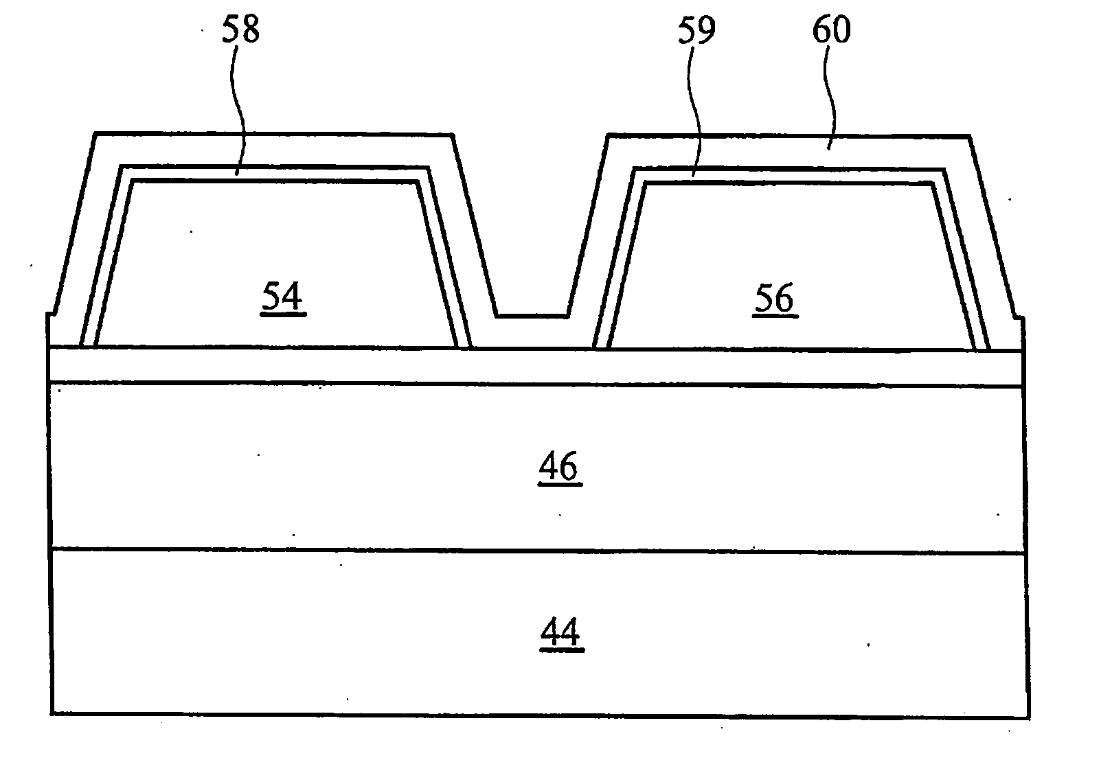
[0009] The present invention provides a method of fabricating multiple-gate MOSFETs that reduces the need for overetching to remove the residue of subsequently deposited material from the fins of such transistors. Subsequently, coatings can be deposited with less variation in thickness over the surfaces of the fins using the techniques of the present invention. A more even level of doping between the tops and sidewalls of the fins can be achieved with traditional ion implantation angles by employing the present invention, which also reduces the need for additional steps in depositing an inter-layer dielectric coating.

Problems solved by technology

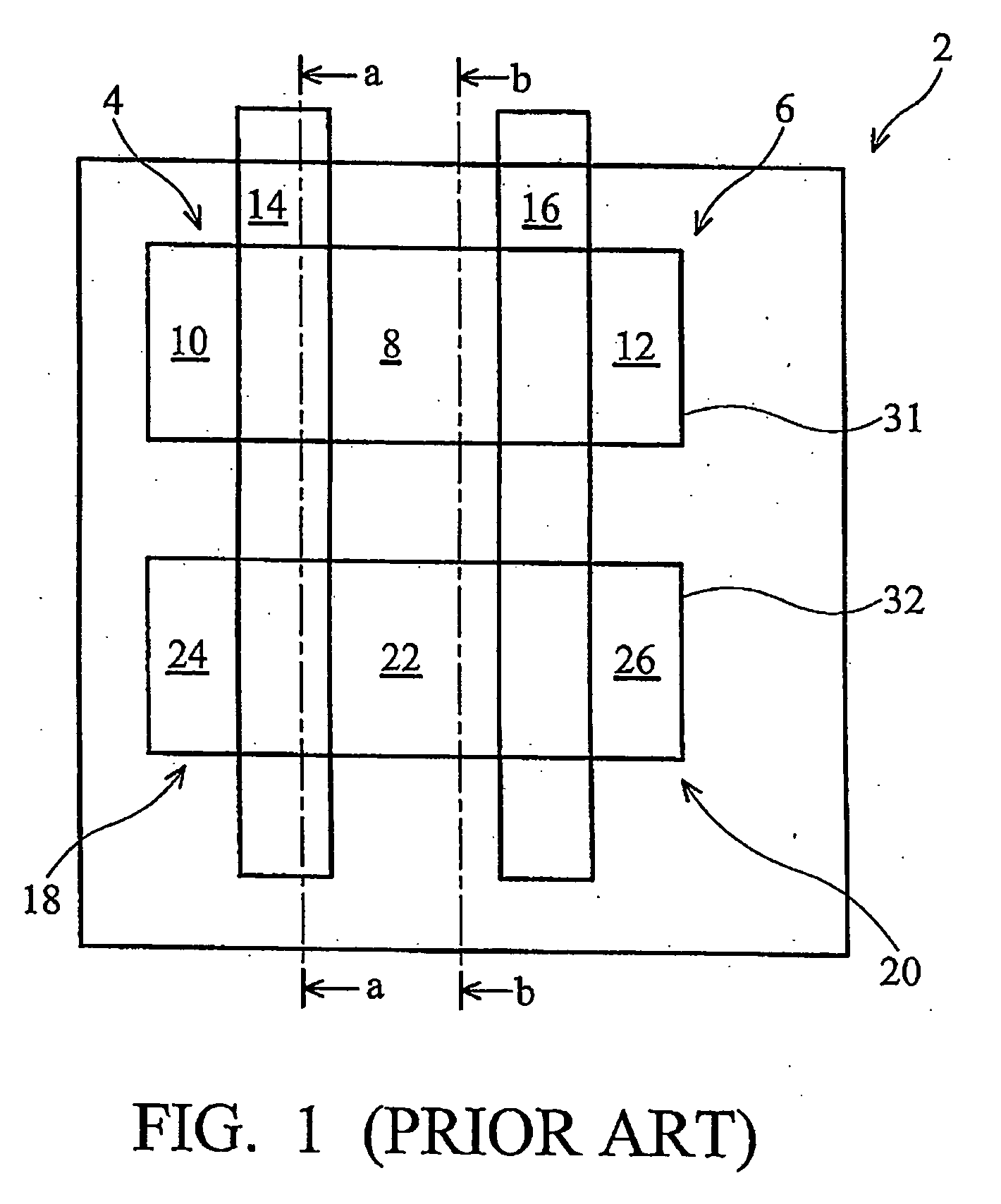
Note that it is undesirable to have polysilicon remaining over the common source / drain regions (or over any regions that are not overlying the channel regions).
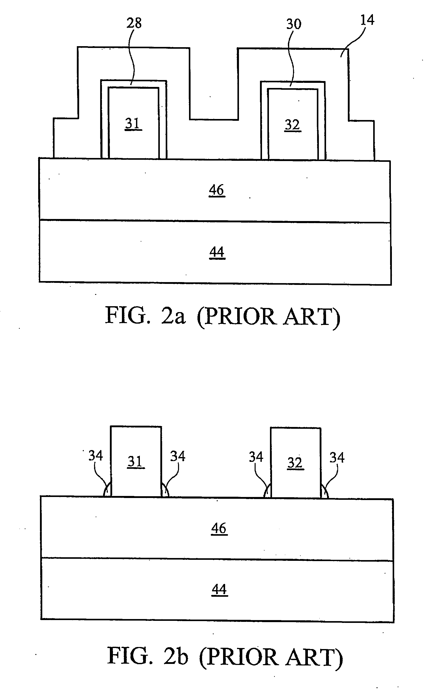
Because of the vertical sidewalls of mesas 31 and 32, however, it is quite difficult to completely remove all of the polysilicon layer during the etching process.
This over-etching, however, can damage the mesa region in which the source / drain regions will be formed, or may damage the underlying gate dielectric.
It is difficult to uniformly dope the sidewall portions of the source / drain regions without using an oblique implantation angle.
Additionally, when mesas are formed orthogonally to one another, an oblique implantation angle could result in dopants being driven into the channel region, thus degrading device performance.
This dual-step approach causes additional process steps that add to the cost and decrease overall yield, however.

Method used


Image

  • Apparatus and method for multiple-gate semiconductor device with angled sidewalls
  • Apparatus and method for multiple-gate semiconductor device with angled sidewalls
  • Apparatus and method for multiple-gate semiconductor device with angled sidewalls

Examples


Embodiment Construction

[0025] The making and using of the presently preferred embodiments are discussed in detail below. It should be appreciated, however, that the present invention provides many applicable inventive concepts that can be embodied in a wide variety of specific contexts. The specific embodiments discussed are merely illustrative of specific ways to make and use the invention, and do not limit the scope of the invention.

[0026] The present invention will be described with respect to preferred embodiments in a specific context, namely a MOSFET device having an active region with a trapezoidal cross-section. The invention may also be applied, however, to other semiconductor devices and other cross-sectional profiles.

[0027]FIG. 4 illustrates a cross-sectional view of a semiconductor substrate 42 that is employed in illustrative embodiments of the present invention. The SOI substrate 42 includes a substrate layer 44 (e.g., silicon, a silicon compound, glass, or quartz), an insulator layer 46 (...


PUM


Abstract

A multiple-gate transistor has an active region with a side that forms an interior angle with the base of the active region of less than 80°. A process for fabricating a FinFET includes the steps of etching a silicon-on-insulator wafer to form an active region, including the source, channel, and drain, with vertically angled sidewalls.

Description

TECHNICAL FIELD [0001] The present invention relates generally to semiconductor devices, and more particularly to multiple gate semiconductor devices having an active region formed in an active layer mesa, the mesa having sloped sidewalls. BACKGROUND [0002] The dominant semiconductor technology used for the manufacture of ultra-large scale integrated (ULSI) circuits is the metal-oxide-semiconductor field effect transistor (MOSFET) technology. A MOSFET consists of source and drain regions separated by a channel region. Current flow between the source and drain through the channel is controlled by a voltage applied to a gate electrode lying adjacent to the channel and separated from it by an oxide dielectric. Traditionally, the source, channel and drain were embedded in a silicon substrate. The oxide dielectric was formed on the upper surface of the channel region, and the gate electrode was deposited on top of the oxide. Efforts to scale MOSFETs into the sub-50-nanometer (nm) regime ...

Claims


Application Information

Patent Timeline
IPC IPC(8): H01L21/336H01L21/84H01L27/01H01L27/12H01L29/10H01L29/40H01L29/786
CPCH01L21/84H01L27/1203H01L29/78684H01L29/7842H01L29/7853H01L29/66795
Inventor LIAW, JHON-JHY
Owner TAIWAN SEMICON MFG CO LTD
Learn More