Printed circuit board manufacturing method and printed circuit board

a manufacturing method and printed circuit board technology, applied in the direction of printed circuit aspects, printed element electric connection formation, conductive pattern formation, etc., can solve the problems of difficult to reliably perform etching, disadvantage of fine line formation, and thickening of the entire metal layer, so as to reduce the depth of the via hole on the land, improve the effect of thickness and finer material

Inactive Publication Date: 2008-10-23
GLOBALFOUNDRIES INC
View PDF9 Cites 10 Cited by
  • Summary
  • Abstract
  • Description
  • Claims
  • Application Information

AI Technical Summary

Benefits of technology

[0017]A printed circuit board according to the present invention includes, in its outline, an insulating substrate having a front surface and a back surface, lines of metal foil selectively formed on the front surface and the back surface, lands selectively formed on the front surface and the back surface, each land being formed of a stack of the metal foil and a plating layer, a dielectric layer formed on an exposed portion and the lines on each of the front surface and the back surface of the insula

Problems solved by technology

If plating is performed on the metal conductor layer in an area where lines will be formed, the entire metal layer becomes thick and it is difficult to reliably perform etching so that the lines have a predetermined line and a line spacing.
This is a disadvantage to forming of fine lines.
If the insulating layer is a prepreg containing glass cloth, the thickness of the insulating layer is limited by the thickness of the glass cloth and cannot be reduced.
If the diameter of the via holes is reduced, the aspect ratio of the via holes becomes higher and the plating liquid cannot flow smoothly to the bottom of each via hole.
As a result, the plating layer at the bottoms of the via holes is made nonuniform in thickness and there is a possibility of occurrence of a crack in the plating layer at the reflow temperature at the time of mounting or in a thermal cycle test and, hence, a possibility of failure to establish interlayer connection.
This is a disadvantage to forming of fine lines.
As described above, it is difficult to reliably perform plating on via holes and to form fine lines.
Also, at the time of etching for forming the lines, failure to completely performing etching may occur due to variation in thickness of the plating layer and there is a po

Method used


Image

  • Printed circuit board manufacturing method and printed circuit board
  • Printed circuit board manufacturing method and printed circuit board
  • Printed circuit board manufacturing method and printed circuit board

Examples


Embodiment Construction

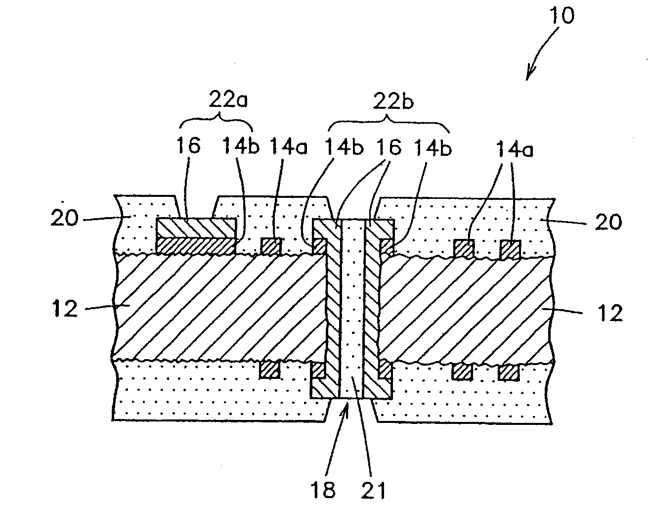
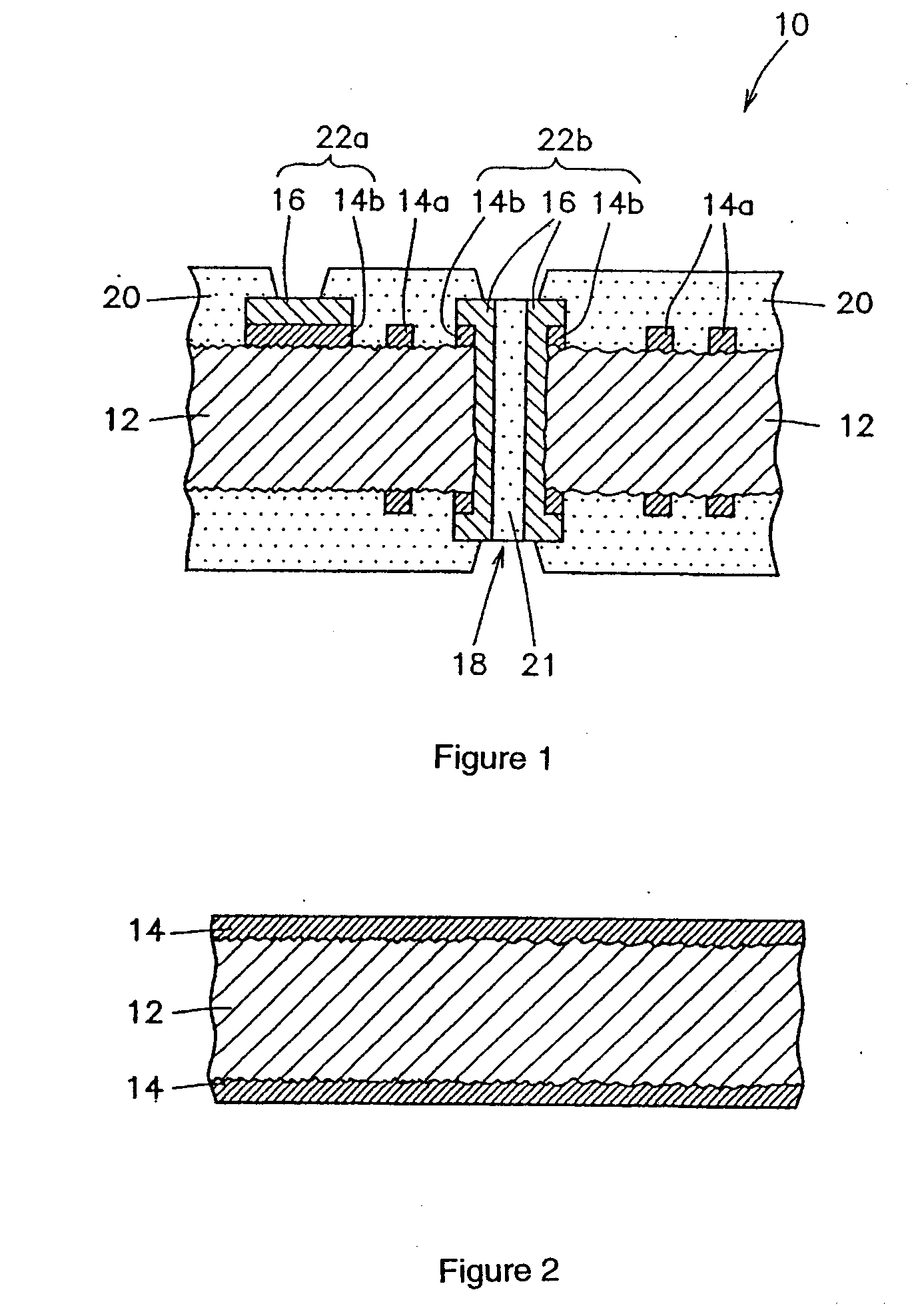
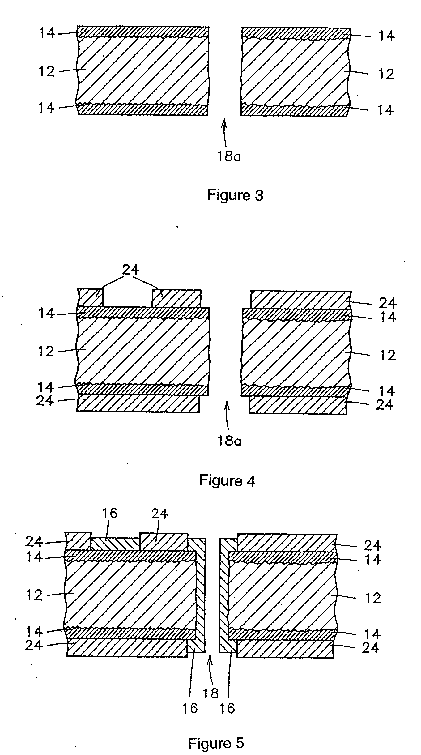
[0043]A printed circuit board manufacturing method and a printed circuit board manufactured by the manufacturing method will be described with reference to the drawings. In a printed circuit board 10 shown in FIG. 1, lands 22a and 22b and lines 14a selectively formed on the front and back surfaces of an insulating substrate 12 differ in thickness from each other. The thickness of the lands 22a and 22b is larger than the thickness of the lines 14a. In the specification and the drawings, lands 22a represent via hole lands, while lands 22b represent through hole lands.

[0044]The lines 14a are formed by processing metal foil 14a on the insulating substrate 12v of the printed circuit board 10. The method of processing metal foil 14a is etching described below, or the like. Metal foil 14 is copper foil or the like. The lands 22a and 22b are formed of a stack of foil 14b and a plating layer 16 on the metal foil 14b. The plating layer 16 is formed by copper plating or the like.

[0045]A layer ...


PUM

PropertyMeasurementUnit
Thicknessaaaaaaaaaa
Thicknessaaaaaaaaaa
Thicknessaaaaaaaaaa

Abstract

The present invention provides a method of manufacturing printed a circuit board capable of formation of via holes having a low aspect ratio and formation of fine lines, and a printed circuit board manufactured by the method. The method of manufacturing a printed circuit board 10 according to the present invention includes a step of selectively forming a plating layer 16 for lands 22a and 22b on a metal foil 14 on the printed circuit board 10, a step of adjusting the thickness of the plating layer 16, and a step of forming the metal foil 14 into lines 14a. The aspect ratio of via holes 28 formed on lands 22a and 22b can be adjusted by adjusting the thickness of the lands 22a and 22b.

Description

CROSS-REFERENCE TO RELATED APPLICATION[0001]The present application is a divisional application of U.S. patent application Ser. No. 10 / 709,752, filed May 26, 2004 and entitled “Printed Circuit Board Manufacturing Method and Printed Circuit Board”.FIELD OF THE INVENTION[0002]The present invention relates to a method of manufacturing a printed circuit board capable of adjustment of the aspect ratio of via holes and to a printed circuit board manufactured by the manufacturing method.BACKGROUND OF THE INVENTION[0003]In recent years, the pitch between terminals of semiconductor chips such as BGA (ball grid array) packages has been reduced. There is a need to reduce the pitch between lines / lands provided on printed circuit boards for mounting of semiconductor chips as well as to reduce the diameter of via / through holes.[0004]A land is a round or polygonal element of a circuit pattern provided on an insulating substrate for a printed circuit board. Terminals of a semiconductor chip are con...

Claims


Application Information

Patent Timeline
IPC IPC(8): H05K1/11H05K3/06H05K3/10H05K3/42H05K3/46
CPCH05K3/064H05K3/108H05K3/427Y10T29/49165H05K2201/0959H05K2203/1394Y10T29/49155H05K3/4602
Inventor OHSUMI, KOHICHITERADA, KENJIYAMAZAKI, KOHICHI
Owner GLOBALFOUNDRIES INC
Why Eureka
Try Eureka