Aligned nanostructure thermal interface material

a thermal interface and nanostructure technology, applied in nanoinformatics, light and heating apparatus, transportation and packaging, etc., can solve the problems of limiting the performance factor of many engineering systems, forming small air gaps, and restricting the flow of thermal energy across the interface, so as to achieve the effect of widening the gap

Inactive Publication Date: 2005-11-17
BRINK DAMON
View PDF5 Cites 77 Cited by
  • Summary
  • Abstract
  • Description
  • Claims
  • Application Information

AI Technical Summary

Benefits of technology

[0019] In another embodiment, the invention is a method of making a thermal interface material for an electronic assembly including depositing conductive structures on a surface, embedding the conductive structures in a matrix material and, aligning the conductive structures using an electric field. In one version, the conductive structures overlap along their length allowing for wider gaps to be spanned. In another version, the conductive structures are longer than the gap to be spanned to allow for thermal expansion and contractions. In a version the number of internal interfaces between the matrix and conducting structures is four or fewer. In another, the number of internal interfaces between the matrix and conducting structures is two or fewer. In all the above embodiments, the conductive structures may be, but not limited to, carbon nanotubes, silver carbon nanotubes, silver nanofibers, or aligned contiguous conductive particles, and matrix material may be, but not limited to thermal grease, silicone, gels, or phase change material.

Problems solved by technology

The transfer of thermal energy is often a limiting performance factor for many engineering systems.
In other words, asperities on the surfaces of the heat spreader and microprocessor result in the formation of small air gaps which act as thermal insulators.
The actual amount of true contact area between the surfaces is quite small, severely restricting the flow of thermal energy across the interface.
Although the use of thermal interface materials substantially decreases the thermal interface resistance, it remains the largest portion of the overall thermal resistance and continues to pose a problem to next generation chip sets which will generate higher thermal loads.
As the thermal expansion coefficients of the components are not all equal, mismatch along the interfaces can occur and results in shearing of the thermal interface material.
These factors can result in large relative displacements between the edge of the microprocessor and the heat spreader.
If the thermal interface material cannot accommodate these displacements, large stresses at the interface can result and cause failure along the interface or within the microprocessor.
Pump-out is caused from a change in the bond-line thickness of the thermal interface that results from distortion of the interface.
This distortion is a direct result of the forces caused by thermal expansion, primarily between the PCB and heat spreader.
The repeated change in TIM volume due to this distortion can result in pump- out.
The aforementioned thermal expansion can present a large problem with metal attach, however.
The large cyclic stresses that can develop often results in thermomechanical fatigue of the metal interlayer, causing the formation of cracks 76 which degrade thermal performance with time resulting in package failure.
Packaging and assembly of the integrated heat spreader and heat sink also presents challenges to the microprocessor industry.
There are often problems with dispensing the paste for TIM 1 that can result in unacceptable variation in the ultimate thermal performance of the assembly.
In addition, there are commonly gaps on the interface that is joined with the paste that act to decrease the heat-carrying capacity of the system.

Method used


Image

  • Aligned nanostructure thermal interface material
  • Aligned nanostructure thermal interface material
  • Aligned nanostructure thermal interface material

Examples


Embodiment Construction

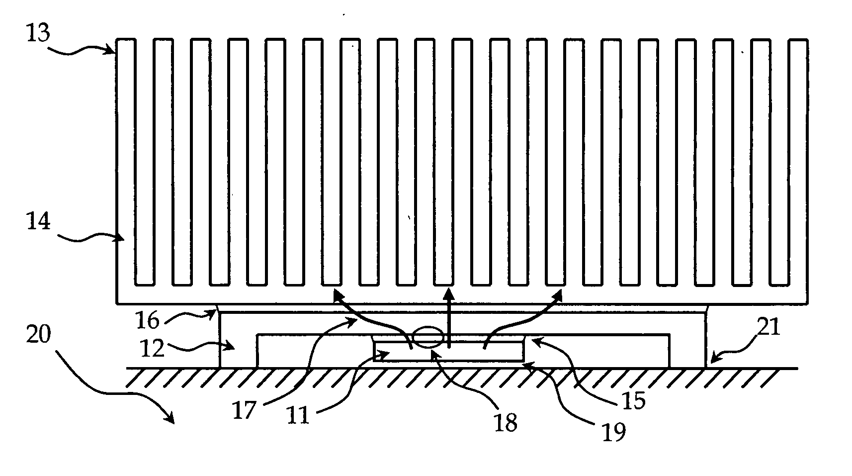
[0031]FIG. 1 depicts a typical thermal packaging solution for a microprocessor used on a desktop computer. In this “flip-chip” configuration, the relevant components include the microprocessor 11, an integrated heat spreader 12, a heat sink 13, the interfaces between these components 15, 16, and the printed circuit board (PCB) substrate 20. Heat generated by the microprocessor during operation is conducted into the heat spreader 12 and subsequently into the heat sink 13 via the interfaces separating these components.

[0032] Continued increases in the processing power of the microprocessor may become limited by the ability to disperse heat, and it is thus beneficial to have a low thermal resistance between the microprocessor and the heat sink. The overall thermal resistance of the package is dominated by the resistance of the interfaces 15, 16, and large performance gains can be realized if the contact resistance associated with these interfaces can be reduced. Although the interfacia...


PUM

PropertyMeasurementUnit
thermalaaaaaaaaaa
conductiveaaaaaaaaaa
electric fieldaaaaaaaaaa

Abstract

The invention relates to a thermal interface material comprising aligned nanostructures to increase the thermal conductivity of an electronic assembly. Aligned carbon nanotubes are a particularly suitable nanostructure possessing very high thermal conductivity. The novel use of nanostructures in the invention is particularly applicable to solving the issues of thermal expansion of the electronic assembly over time.

Description

RELATED APPLICATIONS [0001] This application claims priority to provisional application 60 / 571,111, filed May 14, 2004FEDERALLY SPONSORED RESEARCH [0002] Not Applicable SEQUENCE LISTING [0003] Not Applicable BACKGROUND OF THE INVENTION [0004] This invention relates to assemblies which transfer heat and contain an interface separating a “cold” side and a “hot” side. [0005] The transfer of thermal energy is often a limiting performance factor for many engineering systems. The removal of waste heat from microprocessors is one example, and is quickly becoming one of the primary concerns facing the computer industry. The relevant aspects of heat transfer in computers are depicted in FIG. 1, a schematic of a typical “flip-chip” microprocessor configuration used in many desktop computers sold today. In this configuration, thermal energy generated by the microprocessor 11 is transferred to an integrated heat spreader 12 and subsequently to a heat sink 13 that is cooled by forced convection ...

Claims


Application Information

Patent Timeline
Patent Type & Authority Applications(United States)
IPC IPC(8): B32B3/00B32B9/00B32B15/00F28F13/00H01L23/373H01L23/495
CPCB82Y10/00B82Y30/00F28F13/00H01L23/373H01L23/3733H01L2224/73253Y10T428/24917H01L2924/16152H01L2924/01078Y10T428/30F28F2013/006
Inventor BRINK, DAMON
Owner BRINK DAMON
Why Eureka
Try Eureka