Heterobipolar transistor and method of fabricating the same

Active Publication Date: 2006-10-10
FUJITSU SEMICON LTD
View PDF17 Cites 8 Cited by
  • Summary
  • Abstract
  • Description
  • Claims
  • Application Information

AI Technical Summary

Benefits of technology

[0031]According to this invention, the boron contained within the base layer is dispersed into the emitter layer upon forming the emitter layer onto the base layer, a moderate distribution of boron and a moderate pn junction occurs at the interface of the base layer and the emitter layer, and a portion of the boron enters into the emitter layer at a concentration above 7×1017 cm−3. As a result, a heterobipolar transistor having an excellent noise figure, particularly in the high frequency band, can be obtained.
[0032]In the step of forming the p-type base layer according to the present invention, a SiGe mixed crystal film is preferably deposited after the deposition of the SiGeC mixed crystal layer for realizing a higher concentration of boron compared to the concentration of carbon. In this way, boron is able to be dispersed into the emitter layer through the SiGe mixed crystal layer, which does not cont

Problems solved by technology

In the conventional silicon (Si) bipolar transistor, the carrier mobility within silicon is very limited which in turn limits the operational speed of the device.
On the other hand, the integration of a compound semiconductor device onto a silicon substrate is quite difficult; thus, in the conventional high speed communication system, the high frequency circuit that opera

Method used


Image

  • Heterobipolar transistor and method of fabricating the same
  • Heterobipolar transistor and method of fabricating the same
  • Heterobipolar transistor and method of fabricating the same

Examples


first embodiment

[0053]In the following, the heterobipolar transistor according to the first embodiment of the present invention is described.

[0054]FIG. 4 shows the structure of the vapor deposition apparatus 100 used in the present invention.

[0055]In FIG. 4, the vapor deposition apparatus 100 includes a quartz reactor 101 having a graphite susceptor 102 that can rotate freely, and a processing substrate 103 such as a Si (silicon) wafer, which is to be processed in the above apparatus, is placed on the graphite susceptor 102. In this drawing, the graphite susceptor 102 is covered by a SiC film, not shown in the drawing.

[0056]The quartz reactor 101 is connected, via a flange 101A, to a wafer enter / exit part 104, having a gate valve 104A and a load lock chamber 104B, and air is evacuated from the quartz reactor 101 via an evacuation port 104a, which is implemented in the wafer enter / exit part 104. Also, air is evacuated from the load lock chamber 104B via another evacuation port 104b. Additionally, va...

second embodiment

[0080]Next, the configuration and fabrication method of an npn-type heterobipolar transistor according to a second embodiment of the present invention is described.

[0081]FIGS. 9A–9C, 10A–10C, and 11A–11C show the fabrication process of the heterobipolar transistor according to the second embodiment.

[0082]With reference to FIG. 9A, an n-type impurity, for example, P (phosphorous) at a dose of 1×1014 cm−2 and at acceleration energy 300 keV is ion-implanted to the surface of a p-type Si (silicon) substrate31 to form a n+ dispersion region 32. This n+ dispersion region 32 functions as the collector of the heterobipolar transistor.

[0083]Subsequently, an isolation insulating film 33 is formed on an isolation region of the Si substrate 31 using the LOCOS technique and the like. Then, a SiO2 film 35 is formed on the exposed surface of the substrate 31 at a film thickness of 30–100 nm using the CVD technique, and after forming a polysilicon film 36 onto this surface and the insulating film 3...

third embodiment

[0096]In the following, the structure and fabrication method of a heterobipolar transistor according to a third embodiment of the present invention are described with reference to FIGS. 13 through 20.

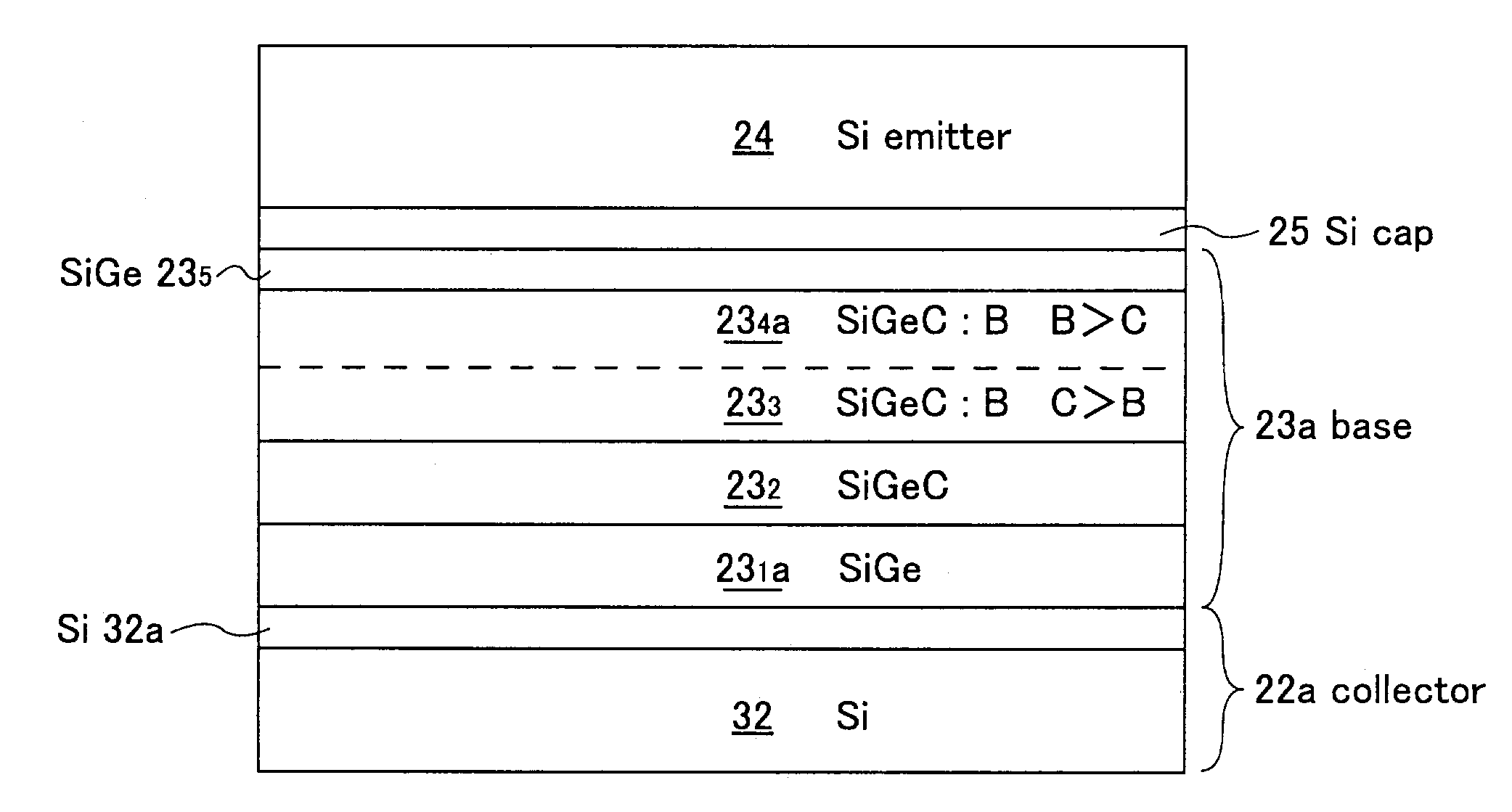
[0097]FIG. 13 is a cross sectional view of the heterobipolar transistor according to the above embodiment. Features / components of the configuration and fabrication method of the heterobipolar transistor of this embodiment that are identical to those of the first and second embodiment described in FIGS. 1 through 12 are given the same numerical references and their descriptions are either simplified or omitted.

[0098]With reference to FIG. 13, the structure of the heterobipolar transistor according to the present embodiment is described in the following.

[0099]As shown, on the p-type Si substrate 31, the n+ well, namely, the n+ type dispersion region 32 is formed. The n+ type dispersion region 32 constitutes a part of a collector layer 22a.

[0100]In the isolation region of the Si substrate...


PUM


Abstract

The present invention realizes a heterobipolar transistor using a SiGeC base layer in order to improve its electric characteristics. Specifically, the distribution of carbon and boron within the base layer is controlled so that the concentration of boron is higher than the concentration of carbon on the side bordering on the emitter layer, and upon the formation of the emitter layer, both boron and carbon are dispersed into a portion of the emitter layer that comes into contact with the base layer.

Description

CROSS-REFERENCE TO RELATED APPLICATIONS[0001]This patent application is based on and claims the benefit of the earlier filing date of Japanese Patent application No. 2002-129062, filed Apr. 30, 2002 and Japanese Patent application No. 2002-271172, filed Sep. 18, 2002, the entire contents of which are hereby incorporated by reference.BACKGROUND OF THE INVENTION[0002]1. Field of the Invention[0003]The present invention relates generally to a semiconductor device and particularly to a high speed semiconductor device having a SiGeC ternary mixed crystal semiconductor layer.[0004]2. Description of the Related Art[0005]Today, the silicon (Si) bipolar transistor is a classic semiconductor device. In the conventional silicon (Si) bipolar transistor, the carrier mobility within silicon is very limited which in turn limits the operational speed of the device. Therefore, a compound semiconductor device employing a compound semiconductor material with large electron mobility in the active regio...

Claims


Application Information

Patent Timeline
IPC IPC(8): H01L31/0328H01L29/06H01L21/331H01L29/10H01L29/24H01L29/732H01L29/737
CPCH01L29/1004H01L29/66242H01L29/7378H01L29/1608
Inventor SATO, HIDEKAZUSUKEGAWA, TAKAESUZUKI, KOUSUKE
Owner FUJITSU SEMICON LTD
Why Eureka
Try Eureka