Junction field effect transistor and method of manufacturing the same

a junction field and transistor technology, applied in the direction of transistors, semiconductor devices, electrical devices, etc., can solve the problems of difficult the inability to achieve the improvement of the high frequency characteristic of the junction fet b>200/b> by reducing the pn junction capacitance, and the inability to manage the variation in the thickness of the epitaxial layer

Active Publication Date: 2008-02-28
SEMICON COMPONENTS IND LLC
View PDF4 Cites 7 Cited by
  • Summary
  • Abstract
  • Description
  • Claims
  • Application Information

AI Technical Summary

Benefits of technology

[0081] Firstly, by forming the channel region by ion implantation, the depth d11 of the channel region can be made shallow. This makes it possible to reduce the area of the pn junctions between the gate region (p type semiconductor layer) and the channel region, as compared to that in the conventional structure. Thereby, the cut-off frequency fT can be improved. As a result, the improvement in the high frequency characteristic of the junction FET can be achieved.
[0082] Secondly, the channel region forms the pn junctions together with the p type semiconductor layer having a lower impurity concentration than that in the conventional structure. Thus, the difference in impurity concentration at the pn junctions between the p type region (p type semiconductor layer) and the edges (side surfaces) of the channel region can be reduced, as compared to the conventional structure (FIG. 8) where the pn junctions are formed between the isolation region, which is a high p type impurity concentration region, and the channel region (well region). By reducing the impurity concentration difference at the pn junctions, the leakage current IGSS can be reduced on each edge of the channel region.
[0083] Thirdly, compared to the conventional structure, the gate region can be made shallow in accordance with the channel region formed shallow. In other words, in order to maintain the IDSS substantially equal to that in the conventional structure, in a case where the depth of the region immediately below the gate region is set to be substantially equal to that in the conventional structure, the gate region can be made shallow by the reduced amount of the depth of the channel region.
[0085] Moreover, when the diffusion depth of the gate region is shallow, the lateral diffusion in the gate region is also reduced. Thus, the distance between the source region and the gate region as well as the distance between the drain region and the gate region can be reduced. As a result, the signal path can be further reduced, contributing to the improvement in the noise figure characteristic of the junction FET.
[0085] Moreover, when the diffusion depth of the gate region is shallow, the lateral diffusion in the gate region is also reduced. Thus, the distance between the source region and the gate region as well as the distance between the drain region and the gate region can be reduced. As a result, the signal path can be further reduced, contributing to the improvement in the noise figure characteristic of the junction FET.
[0086] Fourthly, by forming the conductive layer which comes into contact with the gate region, the gate resistance can be reduced. The gate resistance is an input resistance, and has a large influence on the noise figure characteristic and the distortion characteristic of the junction FET. According to the present invention, the noise figure characteristic and the distortion characteristic can be improved with the reduction in the gate resistance.
[0087] Fifthly, since the epitaxial layer serving as the channel region does not need to be laminated, the cost for wafering is reduced.
[0022] The invention also provides a method of manufacturing a junction field effect transistor. The method includes forming a semiconductor layer of a first general conductivity type on a semiconductor substrate of the first general conductivity type, implanting impurity ions in the semiconductor layer to form a channel region of a second general conductivity type so that a lateral edge of the channel region forms a pn junction with the semiconductor layer, forming a gate region of the first general conductivity type in the channel region, and forming a source region and a drain region that are of the second general conductivity type in the channel region.
[0089] Secondly, the gate region, which is an impurity diffusion region, can be made shallow. In the conventional manufacturing method, the gate region needs to be formed deeply in accordance with the depth of the channel region. Consequently, long heat treatment time is required. In contrast, according to the present invention, the heat treatment time for forming the gate region can be shortened to, for example, ⅓ of the time required in the conventional manufacturing method.

Problems solved by technology

When the layer is made thinner than this limitation, it is hard to manage the variation in thickness of the epitaxial layer 24′ at the time of forming.
Accordingly, there is a problem that characteristics of the channel region 24 are varied.
As a result, the improvement in the high frequency characteristic of the junction FET 200 by reducing the pn junction capacitance cannot be achieved.
In addition, the improvement in the noise figure characteristic of the junction FET 200 has not been achieved either in the conventional structure.
Accordingly, the reduction in the signal path length cannot be achieved.
For these reasons, the internal resistance is increased, and thereby, the noise figure characteristic is deteriorated.

Method used


Image

  • Junction field effect transistor and method of manufacturing the same
  • Junction field effect transistor and method of manufacturing the same
  • Junction field effect transistor and method of manufacturing the same

Examples


Embodiment Construction

[0033] Hereinafter, description will be given in detail of a junction FET according to the present invention with reference to FIGS. 1 to 7.

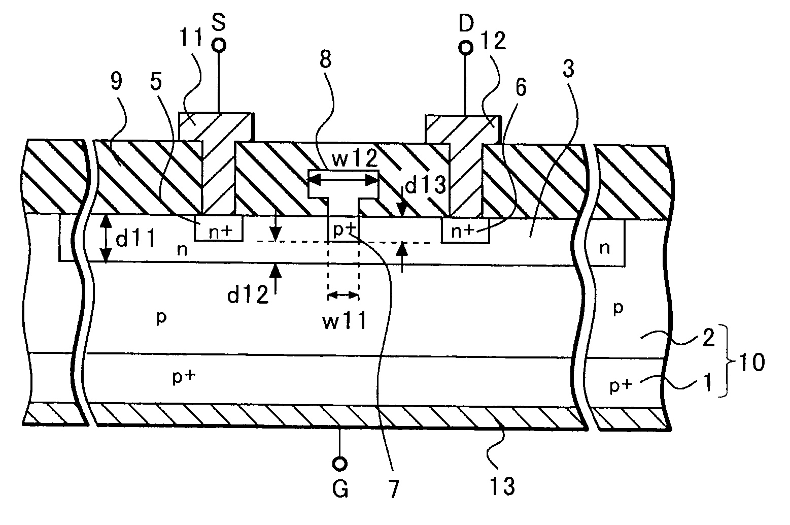
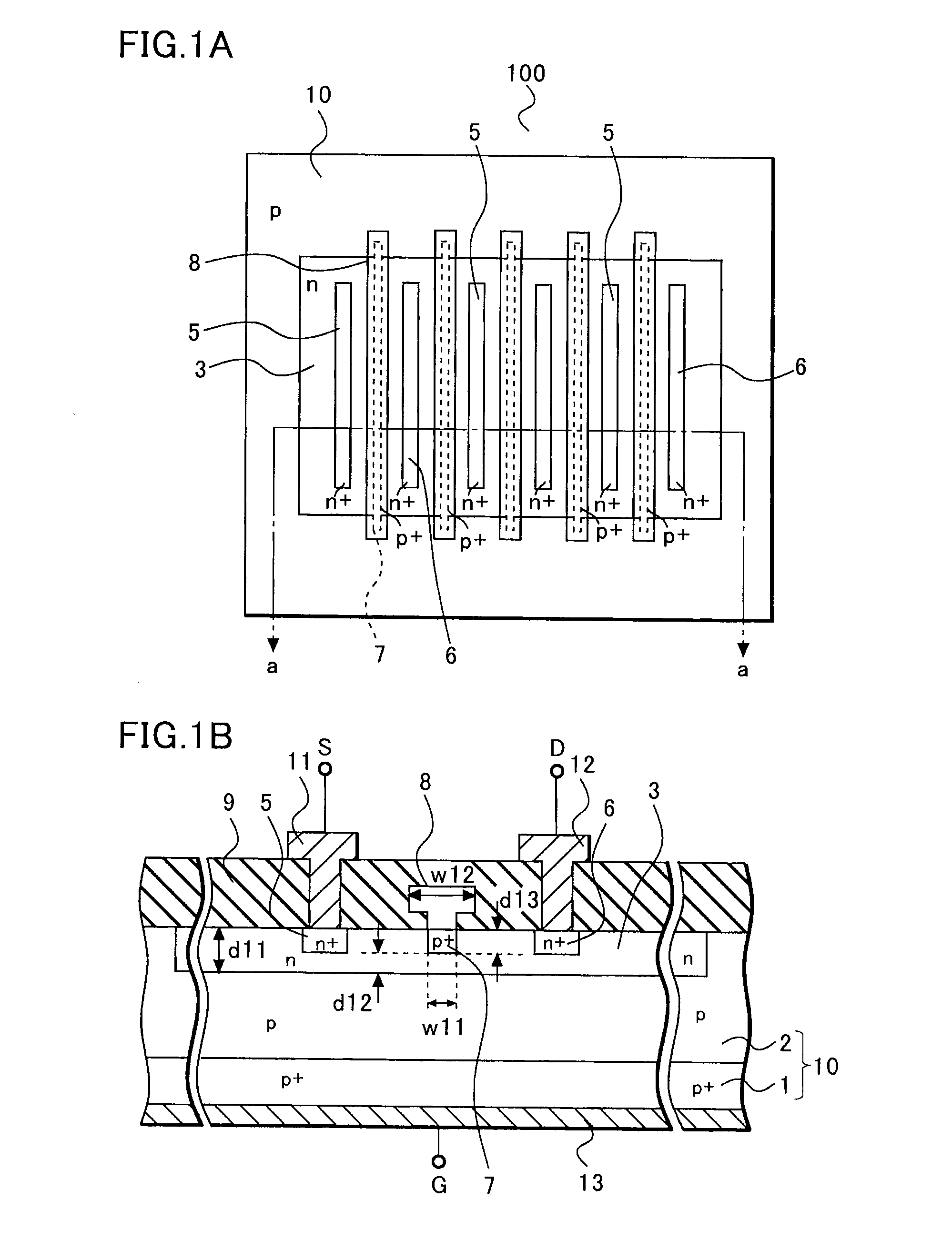
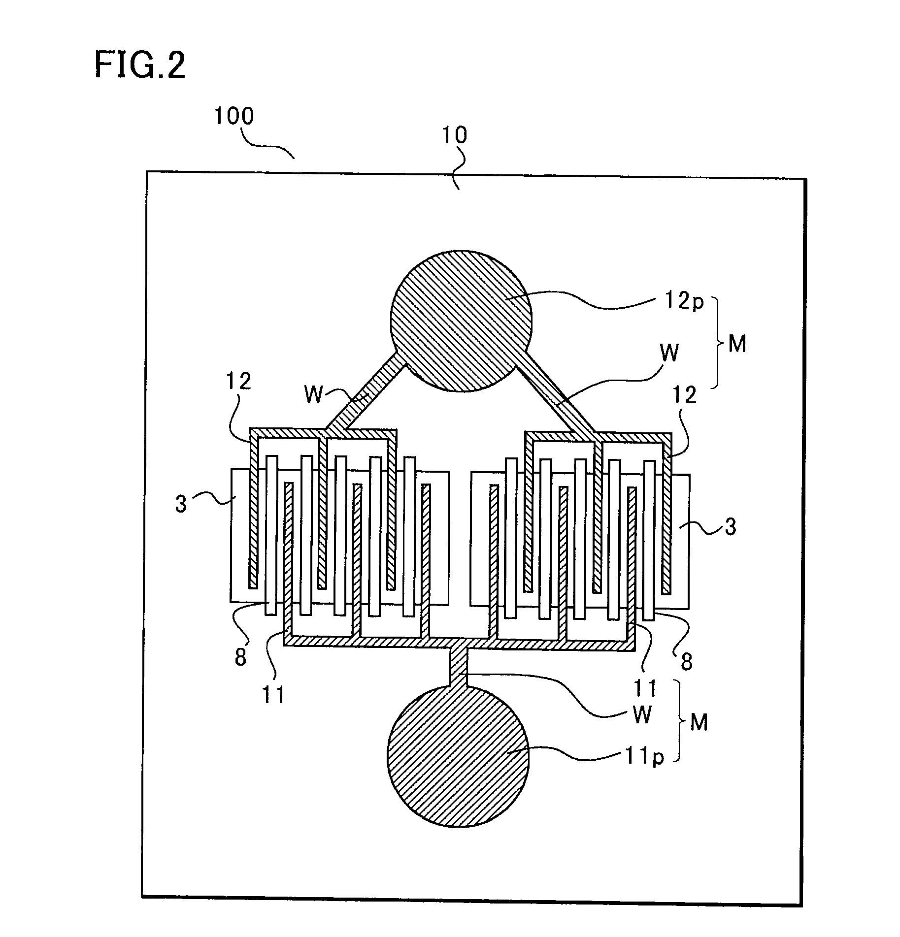
[0034]FIG. 1A and FIG. 1B are views showing a junction FET 100 according to the present embodiment. FIG. 1A is a plan view, and FIG. 1B is a partial cross-sectional view taken along the line a-a in FIG. 1A. Note that, in FIG. 1A, an insulating film and metal electrodes (a source electrode and a drain electrode) provided on the surface of a substrate are omitted. FIG. 1B shows one cell comprised of a source region, a drain region and a gate region.

[0035] The junction FET 100 according to the present invention includes a semiconductor substrate 1, a semiconductor layer 2, a channel region 3, a source region 5, a drain region 6, a gate region 7 and a conductive layer 8.

[0036] As shown in FIG. 1A, the n type channel region 3 is formed in the surface of a p type semiconductor substrate 10. The p type gate regions (shown by chain lines) 7, the n ty...


PUM


Abstract

According to a junction FET of the present invention, the depth of a channel region is made shallow by selectively performing ion implantation and diffusion. Since the channel region forms a pn junction together with a p type semiconductor layer with relatively low impurity concentration, the improvement in the high frequency characteristic and the reduction in the amount of the leakage current because of the reduction in a junction capacitance can be achieved. Moreover, the depth of a gate region is also made shallow by ion implantation, and thus the reduction in noise because of the reduction in the internal resistance can be achieved.

Description

BACKGROUND OF THE INVENTION [0001] This invention claims priority from Japanese Patent Application Number JP2006-229280 filed on Aug. 25, 2006, the content of which is incorporated herein its entirety. [0002] 1. Field of the Invention [0003] The present invention relates to a junction field effect transistor (junction FET) and a method of manufacturing the junction FET, and particularly to a junction FET in which a high frequency characteristic and a noise figure characteristic thereof are improved, and a method of manufacturing the junction FET. [0004] 2. Description of the Related Art [0005] In a conventional junction FET, for example, an n type well region, which serves as a channel region, is formed on a p type semiconductor substrate. In the n type well region, an n+ type source and an n+ type drain regions are formed. Then, a gate region is formed between the source and drain regions. This technology is described, for instance, in Japanese Patent Application Publication No. He...

Claims


Application Information

Patent Timeline
Patent Type & Authority Applications(United States)
IPC IPC(8): H01L29/80H01L21/337
CPCH01L29/1029H01L29/808H01L29/66901H01L29/1066
Inventor KOBAYASHI, SHUNSUKE
Owner SEMICON COMPONENTS IND LLC
Why Eureka
Try Eureka