Heterjunction bipolar transistor with tunnelling mis emitter junction

a technology of emitter junction and heteropolar transistor, which is applied in the direction of transistors, semiconductor devices, electrical equipment, etc., can solve the problems of not being able to completely optimise a conventional transistor for both high speed and high operating voltage, and the device geometry is also affected by the transistor performance, so as to reduce the effect of reducing the probability of electron tunnelling and reducing the number o

Inactive Publication Date: 2006-12-21
EPITACTIX PTY LTD
View PDF5 Cites 10 Cited by
  • Summary
  • Abstract
  • Description
  • Claims
  • Application Information

AI Technical Summary

Benefits of technology

[0047] The present invention, in another aspect, also provides a fabrication means for producing high performance MIS HBT transistors on compound semiconductor substrates. The fabrication process allows emitter structures to be produced with sub-micron dimensions by utilising the metallic emitter layers as a means of connecting the device to other components. This eliminates the need for an additional metal interconnect layer to the emitter which prevents emitter size reduction in conventional devices processes.
[0050] The discovery of the properties of gadolinium oxide when used as a gate dielectric in compound semiconductor MOSFET devices demonstrates that it passivates materials such as gallium arsenide very well. The applicants believe that this dielectric is also suitable for use in other devices such as MIS bipolar transistors where surface passivation is equally important. The bandgap of the insulating material used to form a MIS junction is an important material parameter. If the bandgap is too large e.g. 9 electron volts as for silicon dioxide, the barrier height of the insulator-semiconductor interface reduces electron tunnelling probabilities and junction performance degrades. On the other hand, if the insulator bandgap is too narrow, it is ineffective in stoping unproductive current flow, such as hole current flow from base to emitter in an npn bipolar transistor. Accordingly, it is considered advantageous to use an insulator with a bandgap greater than approximately 3 electron volts
[0051] Furthermore, the invention stems from the realisation that in conventional compound semiconductor HBT, the high surface recombination velocity of electrons in the base-emitter junction creates leakage currents which degrade transistor current gain and increase noise figure. Because the present invention utilises a low-work-function metallic emitter and an insulating barrier through which electrons tunnel, the problems associated with surface leakage currents of conventional devices are eliminated and electrons in the emitter uniformly tunnel through to the base. The MIS structure also enhances the ratio of electron current to hole current flowing from emitter to base because of the favourable band structure of the junction. The resultant MIS structure of the present invention therefore has higher current gain and lower noise figure than conventional compound semiconductor bipolar transistors. The present invention therefore enables compound semiconductor HBT transistors to be manufactured such that they may be reduced in size without compromising their current gain and noise figure. The benefits of this MIS structure could not be realised in prior art compound semiconductor bipolar transistors because a suitable insulating material for the MIS junction was unknown.
[0054] simplifies fabrication requirements and increases device and circuit yields,
[0057] enhances electron transport through the device and improves emitter efficiency, current gain, noise figure and maximum operating frequency. Depending upon the embodiment, one or more of these benefits may be achieved.

Problems solved by technology

Although there have been significant improvements in conventional devices, many limitations still exist and additional improvement is desired.
Therefore, in general, it is not possible to completely optimise a conventional transistor for both high speed and high operating voltage.
Transistor performance is also affected by device geometry.
A major problem is often encountered in the conventional process, however.
These parasitic junctions are a significant problem which limits device and circuit yields in the conventional HBT fabrication.
Manufacturers of conventional HBTs also experience problems in making connections to emitter contacts because they are vertically displaced from the insulating plane on which metal interconnects are deposited on the wafer, as shown in FIG. 4.
These connections can be partially unsupported 407 and fragile which limits device fabrication yields.
This reduces the vertical profile of the transistors and lessens the problems described above, but does not overcome them.
This limits conventional device scaling to around 1 micron emitter widths and prevents improvement of transistor high frequency performance by making devices smaller.
As such transistors are made smaller to enhance their high frequency performance, their gain, efficiencies and noise figures suffer.
The complexity of the processes required to form the emitter mesa and surrounding ohmic and interconnect structures significantly compromises device and circuit fabrication yield.

Method used


Image

  • Heterjunction bipolar transistor with tunnelling mis emitter junction
  • Heterjunction bipolar transistor with tunnelling mis emitter junction
  • Heterjunction bipolar transistor with tunnelling mis emitter junction

Examples


Embodiment Construction

[0073] In the following detailed description, reference is made to the accompanying drawings which form a part hereof, and in which is shown by way of illustration specific preferred embodiments in which the invention may be practiced. These embodiments are described in sufficient detail to enable those skilled in the art to practice the invention, and it is to be understood that other embodiments may be utilized and that structural, material and electrical changes may be made without departing from the scope of the present invention. The following detailed description is, therefore, not to be taken in a limiting sense, and the scope of the present invention is defined only by the appended claims.

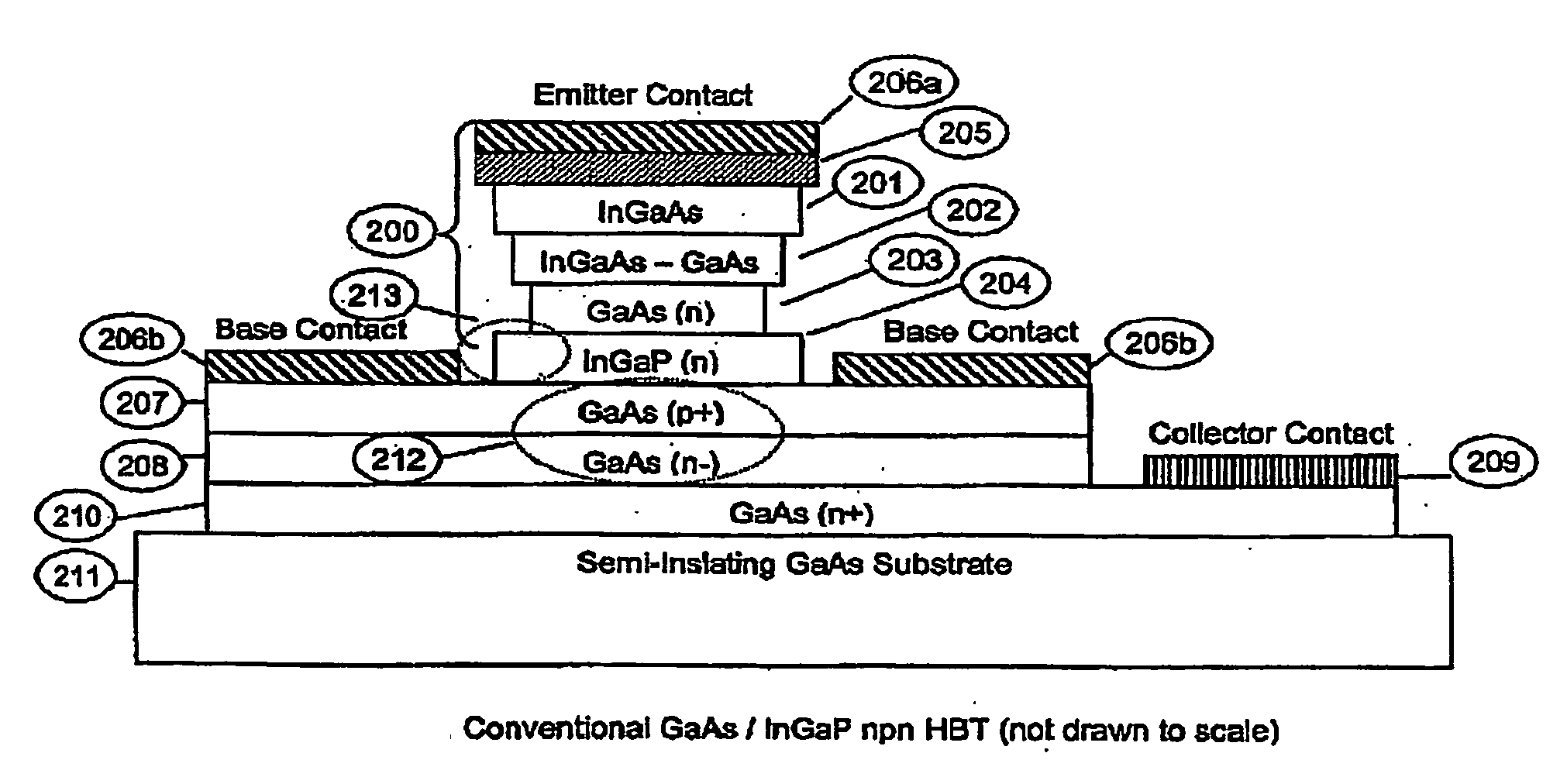
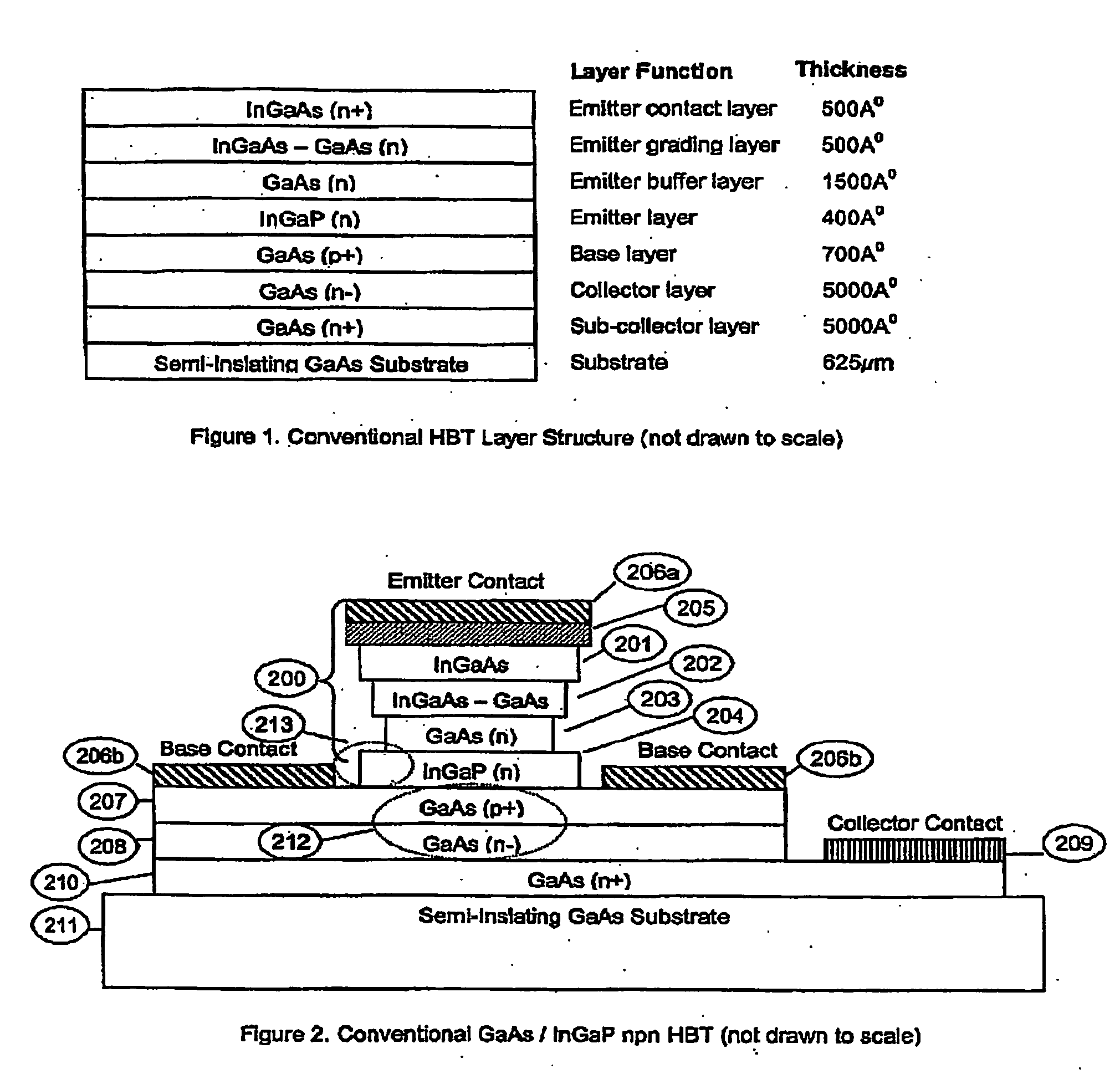
[0074] According to the present invention, improved integrated circuits are provided. More particularly, the invention provides a method and structure for a high performance heterojunction bipolar transistor which is suited to compound semiconductor material systems such as gallium arsenid...


PUM


Abstract

A manufacturing method and structure for a MIS Heterojunction Bipolar Transistor (HBT) is provided including a GaAs substrate which has a collector region; a base layer coupled to the collector region; the ultra-thin insulating layer including a rare earth oxide coupled to the base layer; and an emitter structure including metal layers coupled to the ultra-thin insulating layer.

Description

FIELD OF INVENTION [0001] The present invention relates generally to integrated circuits. More particularly, the invention provides a manufacturing method and structure for a metal-insulator-semiconductor (MIS) transistor structure comprising compound semiconductor material. It will be appreciated, however, that there can be many variations, modifications, and alternatives. It will be convenient to hereinafter describe the invention in relation to a MIS Heterojunction Bipolar Transistor (HBT) comprising a GaAs substrate, however it should be appreciated that the present invention Is not limited to that use only. BACKGROUND [0002] The inventor has identified-the following background and related art. For years, device designers have appreciated the importance of bandgap engineering in designing transistor devices for high performance applications. Bandgap engineering is known as the art of creating semiconductor junctions from materials which have similar crystal structures but differ...

Claims


Application Information

Patent Timeline
Patent Type & Authority Applications(United States)
IPC IPC(8): H01L27/082H01L21/331H01L29/737
CPCH01L29/0817H01L29/0895H01L29/7371H01L29/7311H01L29/66318
Inventor CUNNINGHAM, SHAUN JOSEPH
Owner EPITACTIX PTY LTD
Why Eureka
Try Eureka