Nanometric composites as improved dielectric structures

a dielectric structure and nanometric technology, applied in the field of nanometric composites, can solve the problems of affecting dielectric strength and loss, limiting design, and using fillers such as fillers in a negative way

Inactive Publication Date: 2005-11-17
RENESSELAER POLYTECHNIC INST
View PDF5 Cites 31 Cited by
  • Summary
  • Abstract
  • Description
  • Claims
  • Application Information

AI Technical Summary

Benefits of technology

[0012] It is an object of the present invention to provide a nanometric composite in which internal fields are reduced by a factor up to 10 from conventional composites, and the associated Maxwell-Wagner interfacial polarization is mitigated.
[0013] It is a further object of the present invention to provide a nanometric composite in which filler particles behave cooperatively with the matrix of the composite thereby mitigating the associated Maxwell-Wagner process and reducing interfacial polarization.

Problems solved by technology

In most instances, the dielectric properties of the insulating structure limits the design.
Often the use of such fillers will affect electrical properties, dielectric strength and loss in a negative way.
However, rather surprisingly, the current push to develop nanomaterials based on nanotechnology has not focused much on the opportunities for dielectric materials, but rather centered on optical and mechanical applications, as disclosed in U.S. Pat. Nos. 5,433,906, 5,462,903, 6,344,271, and 6,498,208.
However, the in-filled material will give rise to space-charge accumulation and an associated Maxwell-Wagner polarization due to the implanted interfaces.
Furthermore, macroscopic theories of interfacial polarization do not incorporate a molecular approach since the response is given by relaxation equations if the wavelength is large in comparison with molecular dimensions.
This is because, unlike the strong covalent bonds of elemental crystalline solids, intermolecular binding arises from weak van der Waals' forces that do not allow inter-molecular electronic exchange.

Method used


Image

  • Nanometric composites as improved dielectric structures
  • Nanometric composites as improved dielectric structures
  • Nanometric composites as improved dielectric structures

Examples


example 1

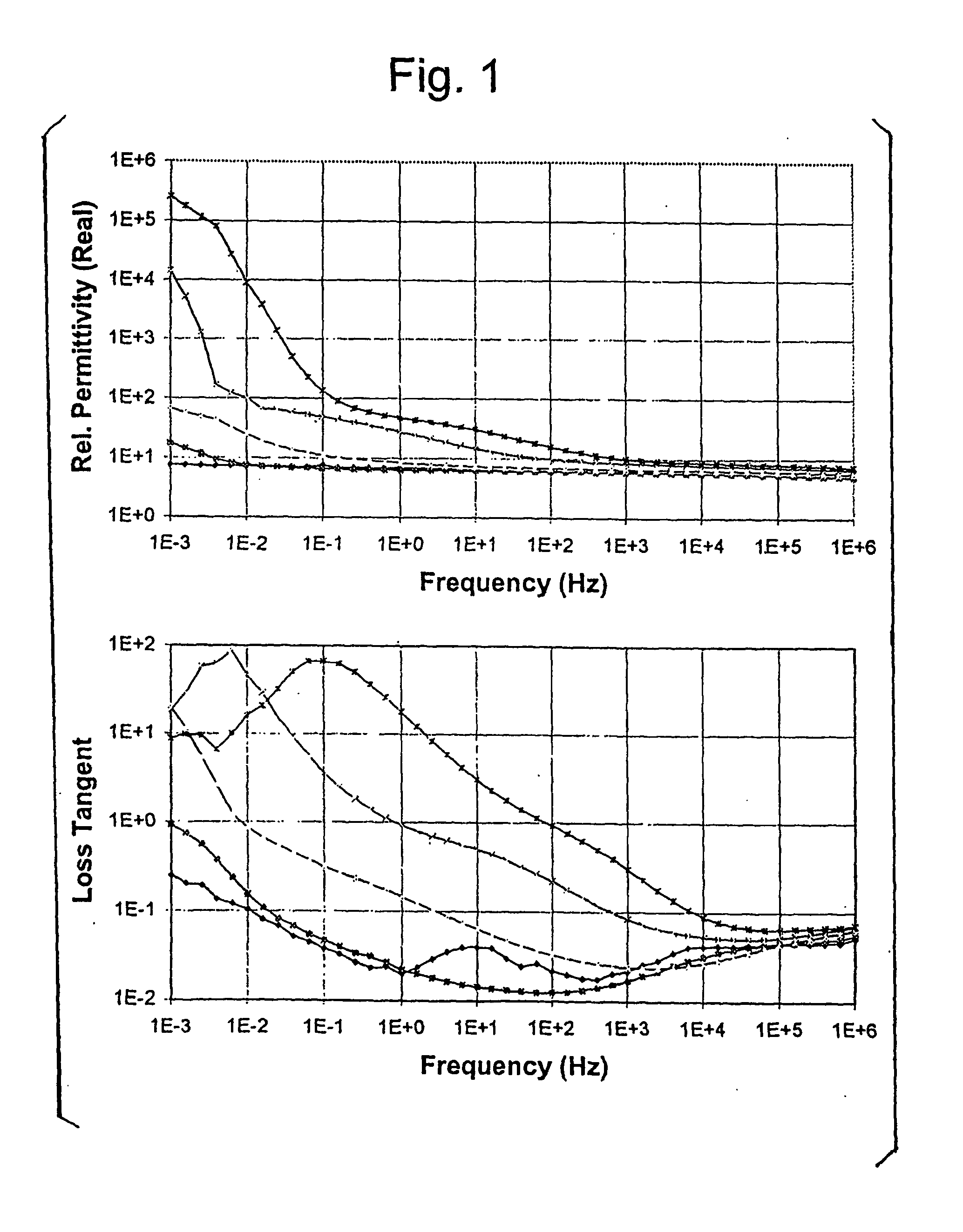
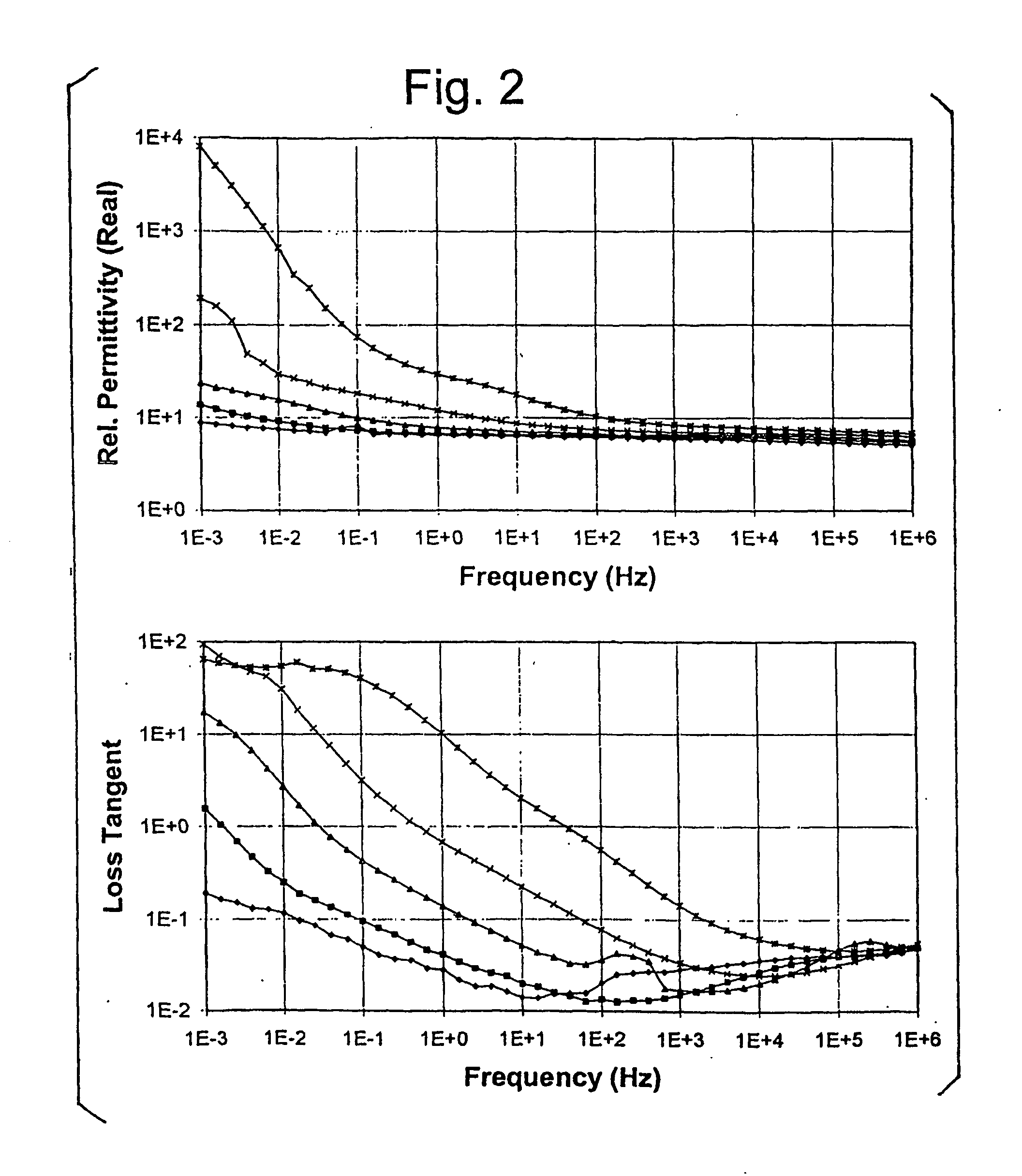
[0039] Composites were provided for micro-particulates and nano-particulates of Titanium Dioxide embedded in a resin matrix of Bisphenol-A epoxy. A list of the composites is shown below in Table 1.

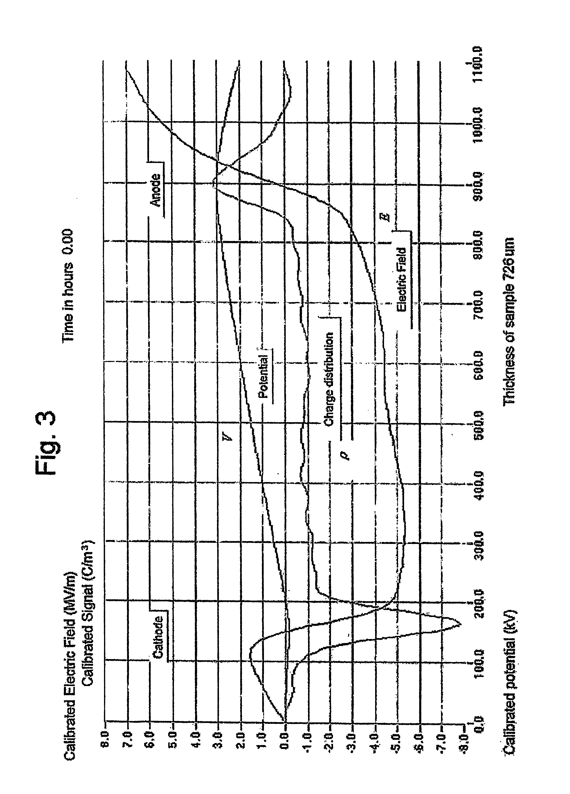
[0040] Test samples of the composites were formed by molding between polished surfaces, held apart by spacers, as described in Griseri V., “The effects of high electric fields on an epoxy resin”, Ph.D. Thesis, University of Leicester, 2000. The molded films range in thickness between 500 and 750 μm. The weighed resin and hardener were degassed at 35° C. and the relevant dried particulate fill was incorporated into the resin by mechanical stirring. Due to their small size, surface interactions for nanoparticles, such as hydrogen bonding, become magnified. This means that the particles tend to agglomerate and dispersion in resins is quite difficult, even in polymers that should be relatively compatible. Hence, in the case of nano-particles, large shear forces are needed in the mixing proces...


PUM

PropertyMeasurementUnit
dielectric constantaaaaaaaaaa
thicknessaaaaaaaaaa

Abstract

A dielectric is provided which possesses high dielectric constant and high dielectric strength, while having the ca-pabilities of a polymer. The dielectric comprises a nanometric composite, which includes a stoichiometric nano-particulate filler embedded in a polymer or resin matrix. Filler particles are reduced in physical size to dimension to the same order as the polymer chain length of the host material and interact cooperatively thereby mitigating the associated Maxwell-Wagner process and reducing interfacial polarization. The internal fields for the new formulation are nearly a factor of 10 lower then for conventional (micro) material. The large changes in the internal field of the composite permit engineering of nanocomposite materials with enhanced electric strength and improved voltage endurance properties.

Description

FIELD AND BACKGROUND OF THE INVENTION [0001] The present invention relates generally to the field of nanometric composites and in particular to a new and useful dielectric structure comprising nanometric composites. [0002] Electrical insulation is a pervasive technology which is a huge commercial business ranging from the thin films used in the microelectronics industry to the large amounts of material used to insulated high-voltage equipment in the power segment of this market. In most instances, the dielectric properties of the insulating structure limits the design. A 20% improvement in performance would thus have significant industrial significance and so the substantial changes that are indicated by this disclosure are believed to be commercially important. [0003] Polymers of many types are commonly used as electrical insulation. The use of conventional fillers for polymer materials is well known and is usually employed to reduce the cost of a material or to modify one of the m...

Claims


Application Information

Patent Timeline
Patent Type & Authority Applications(United States)
IPC IPC(8): C08K3/00C08K3/18H01B3/10H01B3/28H01B3/30H01B3/40H01B3/44
CPCB82Y30/00C08K3/0008C08K2201/011H01B3/441H01B3/28H01B3/306H01B3/40H01B3/10C08K3/01
Inventor NELSON, J. KEITH
Owner RENESSELAER POLYTECHNIC INST
Why Eureka
Try Eureka