Surface treatment method and surface treatment device

Inactive Publication Date: 2005-12-08
PANASONIC CORP
View PDF5 Cites 59 Cited by
  • Summary
  • Abstract
  • Description
  • Claims
  • Application Information

AI Technical Summary

Benefits of technology

[0065] In this way, it becomes possible to perform chemical etching and mechanical polishing at the same time, which makes it possible to realize planarization at a further higher speed.
[0066] As described up to this point, with the surface treatment method and the surface treatment device of the present invention, ultraviolet rays to be irradiated on the electrolyte containing fine metal particles and the nitride semiconductor surface can accelerate the formation of pairs of an electron and a hole on the nitride semiconductor surface and the dissolution of the nitride semiconductor, and thus it becomes possible to perform chemical polishing etching of t

Problems solved by technology

However, in the surface treatment method and the surface treatment device that are conventionally applied for planarization of a GaN suraface, it is impossible to realize an excellent surface planarization at an atom level.
However, it is impossible to easily realize a high-speed planarization because it is generally diffi

Method used


Image

  • Surface treatment method and surface treatment device
  • Surface treatment method and surface treatment device
  • Surface treatment method and surface treatment device

Examples


first embodiment

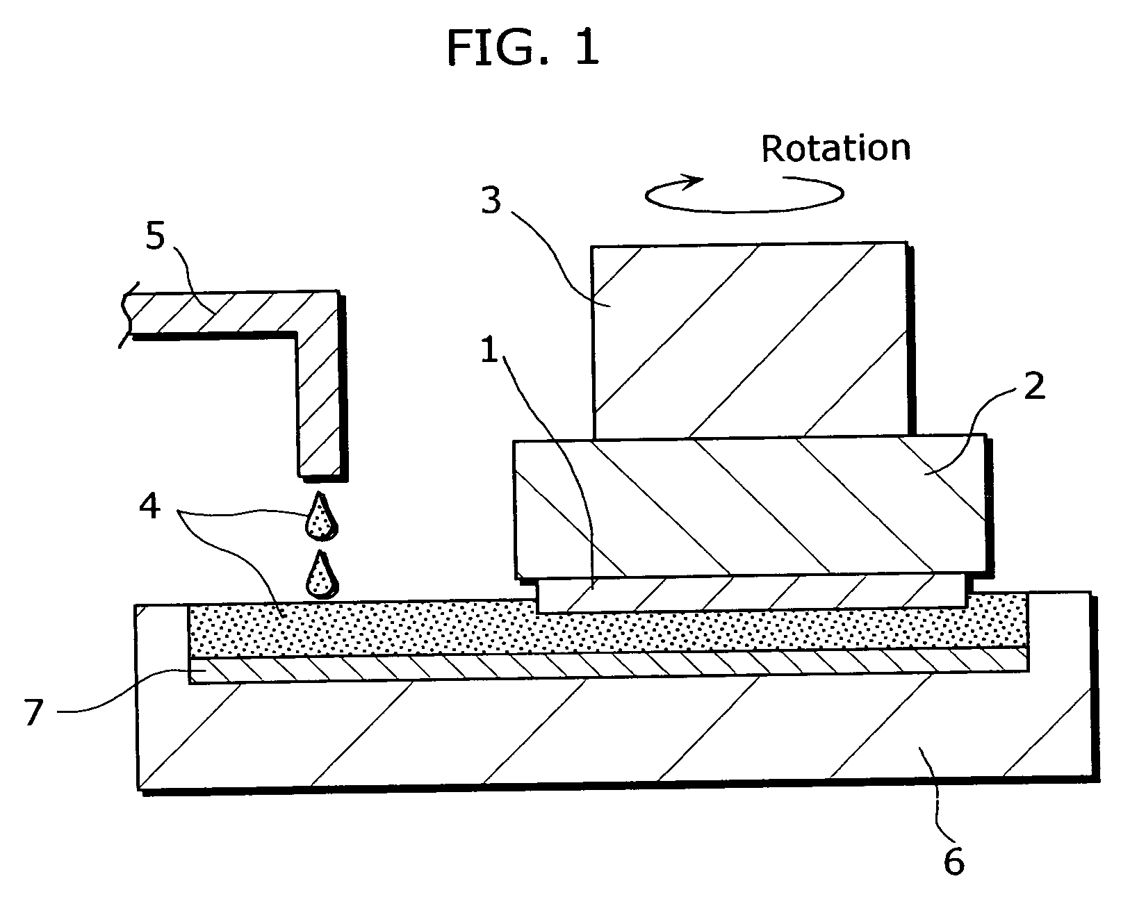
[0077]FIG. 2 is a cross-sectional view of a surface planarization device, showing the structure of the device in a first embodiment of the present invention.

[0078] This surface planarization device is for planarizing the surface of a GaN substrate 11. The surface planarization device includes (i) an electrolyte supply port 15 for supplying a KOH electrolyte 14 that is an alkaline electrolyte containing an abrasive such as fine Pt particles or diamond powder, (ii) a storage container 40 having an opening on the top surface and is for storing the KOH electrolyte 14 supplied from the electrolyte supply port 15, (iii) a wafer holder 12 for fixing and bringing the GaN substrate 11 into contact (become wet) with the KOH electrolyte 14 in the storage container 40 by impregnating the surface of the GaN substrate 11 into the KOH electrolyte 14 from above, (iv) a load 13 that is placed on the wafer holder 12, the load 13 and the wafer holder 12 constituting the contact unit, (v) a device hou...

second embodiment

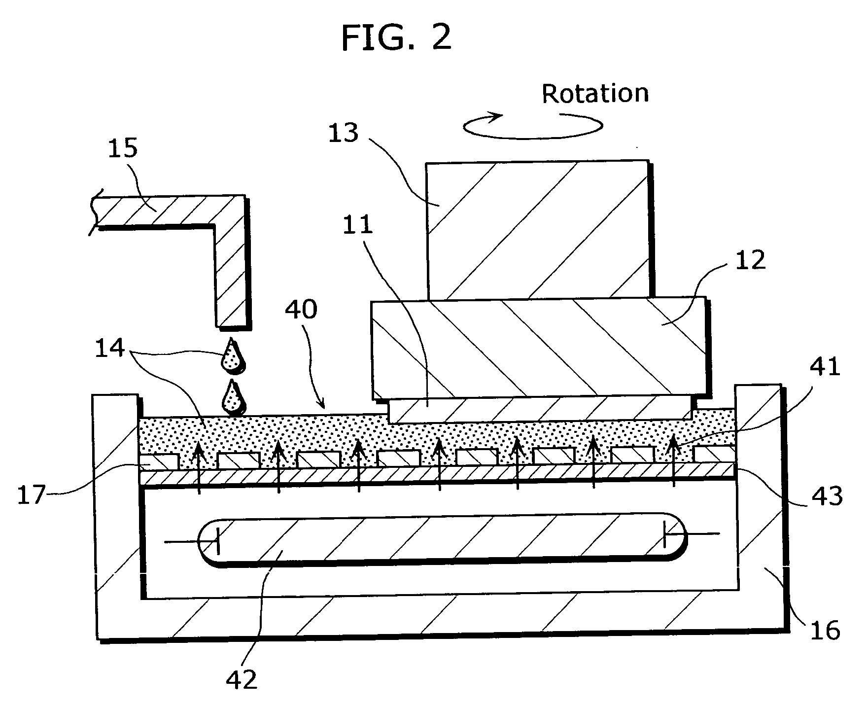
[0092]FIG. 3 is a cross-sectional view of a surface planarization device, showing the structure of the device in a second embodiment of the present invention.

[0093] This surface planarization device is for planarizing the surface of the GaN substrate 51. The surface planarization device includes (i) an electrolyte supply port 15 for supplying a KOH electrolyte 14 including fine Pt particles and an abrasive, (ii) a storage container 40, (iii) a wafer holder 52 for fixing the GaN substrate 51 and bringing the GaN substrate 51 into contact with the KOH electrolyte 14 in the storage container 40 by impregnating the surface of the GaN substrate into the electrolyte 14 from above, (iv) a load 13 that constitutes the contact unit together with the wafer holder 52, (v) a device housing 16, (vi) a polishing pad 44 for polishing the surface of the GaN substrate 51 placed on the quartz board 43 that constitutes the back surface of the storage container 40, (vii) an ultraviolet ray source 42 f...

third embodiment

[0102]FIG. 4 is a cross-sectional view of a surface planarization device, showing the structure of the device in a third embodiment of the present invention.

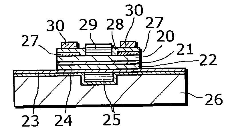
[0103] This surface planarization device is for planarizing the surface of the GaN substrate 51. The surface planarization device includes (i) an electrolyte supply port 15 for supplying the KOH electrolyte 14 including fine Pt particles and an abrasive, (ii) a storage container 40, (iii) a wafer holder 52, (iv) a load 13, (v) a device housing 16, (vi) a polishing pad 67, for polishing the surface of the GaN 51, placed on the back surface of the storage container 40, (vii) a power supply 45 and (viii) electrode pins 46. The GaN substrate 51 is structured by forming a GaN thin film on a sapphire substrate using the MOCVD method.

[0104] The polishing pad 67 is placed facing the surface to be polished of the GaN substrate 51. The polishing pad 67 is an electrically-conductive member made of, for example, a metal board.

[0105] The ...


PUM

PropertyMeasurementUnit
Band gapaaaaaaaaaa
Electric potential / voltageaaaaaaaaaa
Transparencyaaaaaaaaaa

Abstract

The present invention is conceived in order to accomplish an object of providing a surface treatment method and a surface treatment device that can planarize, at high speed, the surface of a nitride semiconductor with an excellent evenness. The surface treatment device includes an electrolyte supply port 15 for supplying a KOH electrolyte 14 containing fine metal particles and an abrasive, a storage container 40 having an opening on the top surface and is for storing the KOH electrolyte 14 supplied from the electrolyte supply port 15, a wafer holder 12 for fixing the GaN substrate 11 and bringing the surface of the GaN substrate 11 into contact with the KOH electrolyte 14 by impregnating the surface of the substrate into the KOH electrolyte 14 in the storage container 40 from above, a load 13 placed on the wafer holder 12, a device housing 16, a polishing pad 17 for polishing the surface of the GaN substrate 11 and an ultraviolet light source 42.

Description

BACKGROUND OF THE INVENTION [0001] (1) Field of the Invention [0002] The present invention relates to a substrate surface treatment method and a substrate surface treatment device that can be applied in manufacturing processes of integration circuits. Integration circuits include a semiconductor laser element, a light emitting diode, a field effect transistor and the like that are made from, for example, a nitride semiconductor. The present invention especially relates to a substrate surface planarization method and a substrate surface planarization device. [0003] (2) Description of the Related Art [0004] A GaN system nitride semiconductor (generally represented as InGaAlN) has a wide band gap, for example, the band gap of GaN at room temperature is 3.4 eV. The material can realize light-emitting diodes with a high power output in the blue and green visible region or within the wavelength range of ultraviolet rays. Such blue and green light-emitting diodes and white high-power-outpu...

Claims


Application Information

Patent Timeline
IPC IPC(8): C25F3/02C25F3/12H01L21/306H01L21/3063H01L27/15H01L33/00H01S5/02H01S5/042H01S5/183H01S5/323
CPCC25F3/02C25F3/12H01L21/30625H01L21/30635H01S5/32341H01S5/0213H01S5/0217H01S5/0425H01S5/18369H01L33/0095H01S5/04252H01S5/04254
Inventor UEDA, TETSUZOUEDA, DAISUKE
Owner PANASONIC CORP
Why Eureka
Try Eureka