Single-stage buck-boost inverter
a power inverter, single-stage technology, applied in the direction of ac network voltage adjustment, automatic controller, electric variable regulation, etc., can solve the problems of nuclear waste disposal, plant safety problems, and new power generation capacity cannot be met by traditional methods such as burning coal, oil, natural gas, etc., to achieve low cost, low component count, and high efficiency power converter
- Summary
- Abstract
- Description
- Claims
- Application Information
AI Technical Summary
Benefits of technology
Problems solved by technology
Method used
Image
Examples
first embodiment
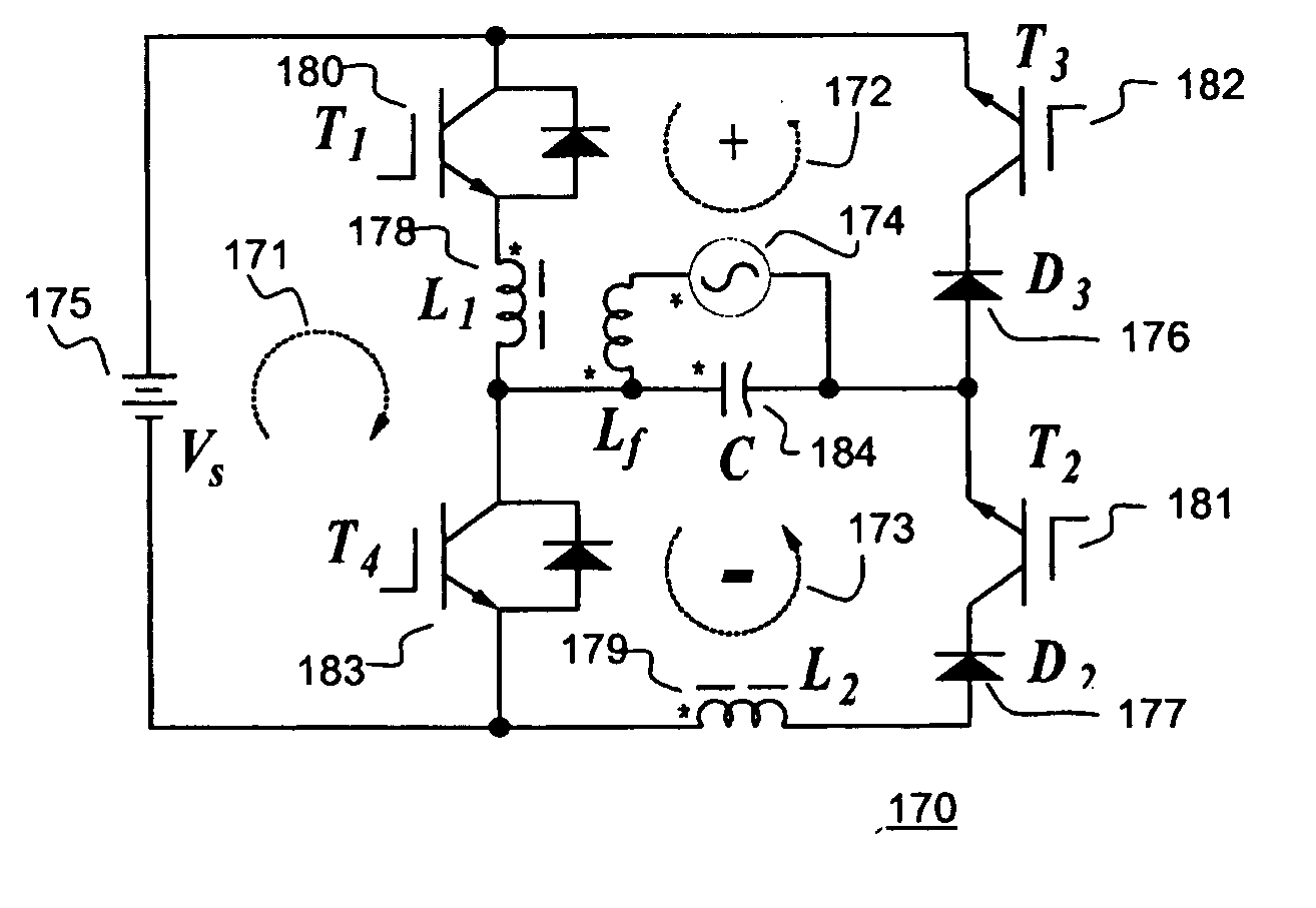
[0051]FIG. 17 is a schematic illustration of the S2B2 inverter 170 of the present invention. It consists of one charge loop 171 (T1 180, L1 178, and T4 183) and two discharge loops 172, 173 (T1 180, L1 178, C 184, D3 176, and T3 182 for the positive half cycle 172; and T4 183, L2 179, D2 177, T2 181, and C 184 for the negative half cycle 173). The reverse power flow from grid 174 to source Vs 175 is blocked by D3 176 and D2 177. The energy-storage components, L1 178 and L2 179, are the primary and secondary windings of a flyback transformer and have identical inductance (L) and number of turns. As is well understood in the art, the switches T1 180, T2 181, T3 182 and T4 183, are controlled by a separate control circuit not illustrated in FIG. 17.
[0052] Each of the functional loops 171, 172, 173 is associated with one of three switch operation modes. Charge loop 171 is used in charge mode, wherein switch T1 180 and T4 183 are on and switch T2 181 and T3 182 are off. An approximate eq...
second embodiment
[0067] the present invention is illustrated in FIG. 26. This single-stage buck-boost inverter 260 uses only three switching devices 261, 262, 263.
[0068] The circuit operation can be divided into four modes. Mode 1 and mode 2 work in positive half cycle, and mode 3 and mode 4 work in negative half cycle.
[0069] Positive half cycle: During mode 1, switching device Q1261 is turned on and switching devices Q2262 and Q3263 are turned off, the coupled inductor L1264 will be charged with input voltage 175; and during mode 2, switching device Q1261 and Q3263 are turned off and Q2262 is turned on, the energy in L1264 will be discharged to the grid through D2266.
[0070] Negative half cycle: During mode 3, switching device Q1261 is turned on again (Q2262 and Q3263 are turned off) and the coupled inductor L1264 will be charged; and during mode 4, switching device Q1261 and Q2262 will turned off and switching device Q3263 will turned on, the energy transferred to the coupled inductor L2265 from ...
PUM
| Property | Measurement | Unit |
|---|---|---|
| peak current | aaaaa | aaaaa |
| peak current | aaaaa | aaaaa |
| operating frequency | aaaaa | aaaaa |
Abstract
Description
Claims
Application Information


