Annealing apparatus, annealing method, and manufacturing method of a semiconductor device
a technology of semiconductor devices and annealing methods, which is applied in the direction of electrostatic spraying apparatus, semiconductor devices, coatings, etc., can solve the problems of high impurity concentration, high impurity concentration, and difficult to form shallow impurity diffusion regions with low resistance, so as to reduce light intensity
- Summary
- Abstract
- Description
- Claims
- Application Information
AI Technical Summary
Benefits of technology
Problems solved by technology
Method used
Image

Examples
first embodiment
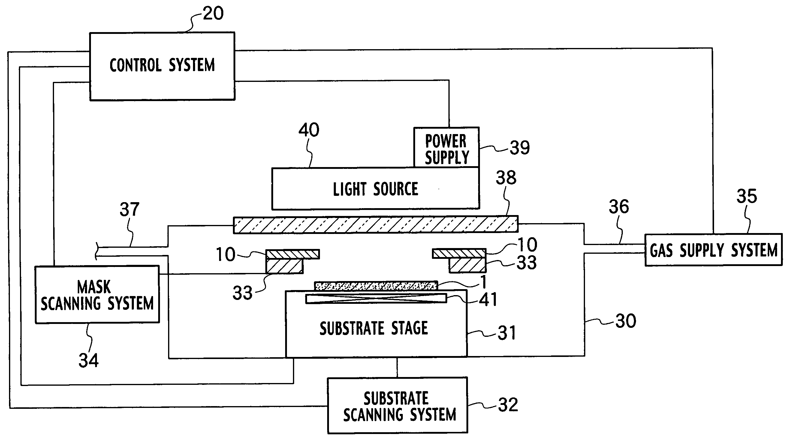
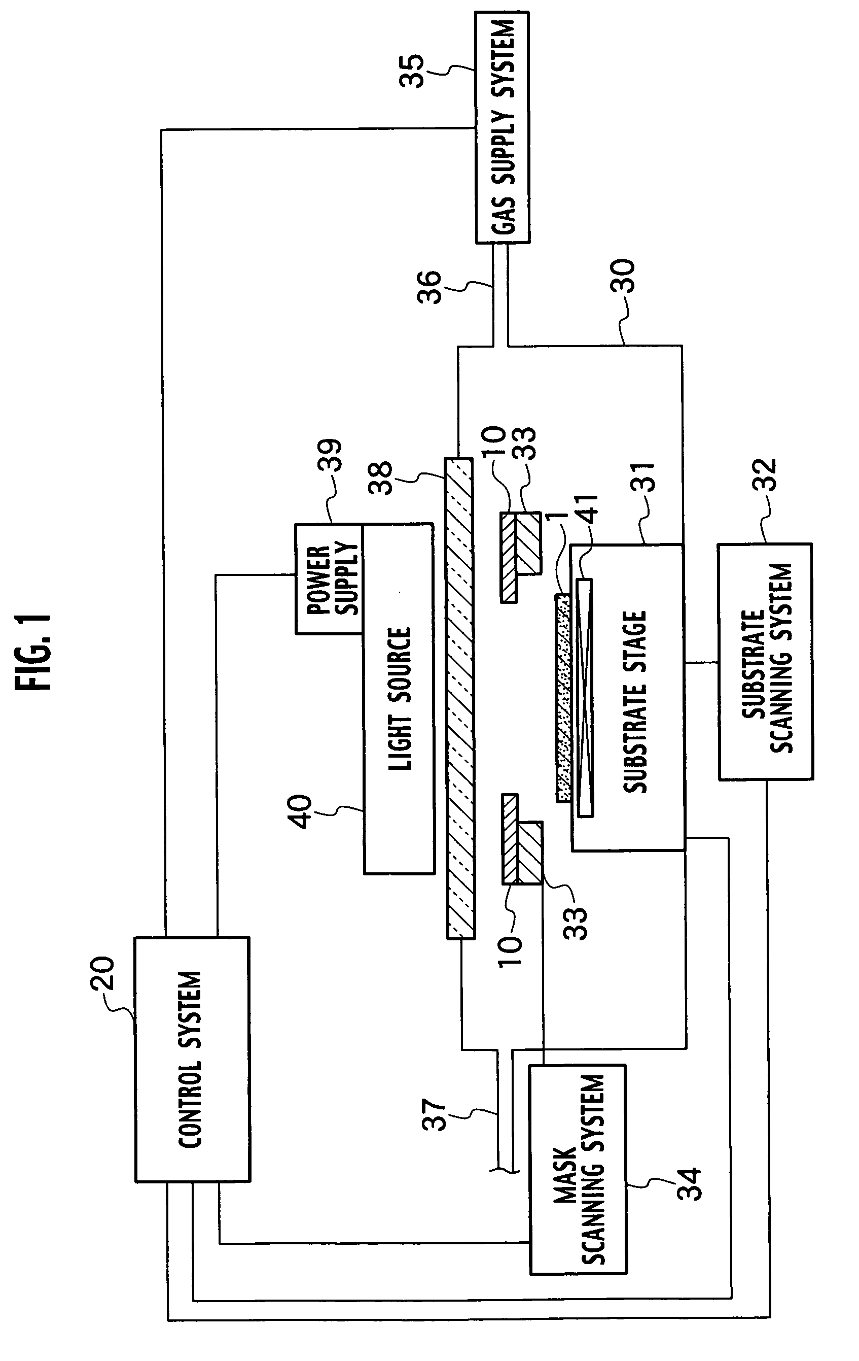
[0038] An annealing apparatus according to a first embodiment of the present invention includes a process chamber 30, a gas supply system 35, a light source 40, and a control system 20. Feeding piping 36 and exhaust piping 37 are provided on the process chamber 30, as shown in FIG. 1. The feeding piping 36 is connected to the gas supply system 35. A transparent window 38 is disposed on top of the process chamber 30 and faces the light source 40. A substrate stage 31, on top of which a semiconductor substrate 1 is placed, is disposed facing the light source 40 on the bottom of the interior of the process chamber 30. A mask 10 is disposed in between the transparent window 38 and the semiconductor substrate 1. A mask stage 33 is disposed inside of the process chamber 30 and the mask 10 is placed on top of the mask stage 33. The substrate stage 31 and the mask stage 33 are connected to a substrate scanning system 32 and a mask scanning system 34 respectively. And a power supply 39 is co...
second embodiment
[0063] In an annealing apparatus according to a second embodiment of the present invention, a mask 110 is provided on the peripheral region of the surface of the semiconductor substrate 1, as shown in FIG. 13. A flash lamp light from the light source 40 is irradiated on the entire surface of the semiconductor substrate 1 having the mask 110. A peripheral region width Wo on which the mask 110 is formed is provided wider than a notch width Wn of a notch 2, as shown in FIG. 14. It is possible to use a light reducing material having a rate of light transmission of below 80%, and a highly reflective metallic film such as Al, silver (Ag), rhodium (Rh), nickel (Ni), platinum (Pt), antimony (Sb), as the mask 110. By the mask 110, the flash lamp light is selectively shielded, or reduced in intensity by over 20% in the peripheral region along the outer edge of the semiconductor substrate 1. Thus, it becomes possible to suppress damage that occurs on the semiconductor substrate 1, and improve ...
third embodiment
[0067] In an annealing apparatus according to the third embodiment of the present invention, a mask 10a is placed on the mask stage 33, as shown in FIG. 17. An rectangular-shaped opening 12a having an opening width WA is provided on the mask 10a, as shown in FIG. 18. Metal such as Al or material that shields light in a wavelength below 1 μm such as SiC is used as the mask 10a. The mask 10a is disposed in such a way that the irradiation region corresponding to the opening 12a is located within the outer edge of the semiconductor substrate 1. The peripheral region along the outer edge of the semiconductor substrate 1 is not irradiated by a flash lamp light. Thus, it becomes possible to suppress damage that occurs on the semiconductor substrate 1, and improve the cracking resistance of the semiconductor substrate 1. In the third embodiment, the aspect in which the mask 10 having the rectangular-shaped opening 12a is used differs with the first embodiment. Other configurations of the th...
PUM
 Abstract
Description
Claims
Application Information
 - Generate Ideas
- Intellectual Property
- Life Sciences
- Materials
- Tech Scout
- Unparalleled Data Quality
- Higher Quality Content
- 60% Fewer Hallucinations
Browse by: Latest US Patents, China's latest patents, Technical Efficacy Thesaurus, Application Domain, Technology Topic, Popular Technical Reports.
© 2025 PatSnap. All rights reserved.Legal|Privacy policy|Modern Slavery Act Transparency Statement|Sitemap|About US| Contact US: help@patsnap.com