Method for manufacturing semiconductor device

a manufacturing method and semiconductor technology, applied in semiconductor devices, capacitors, electrical devices, etc., can solve the problems of capacitor damage, capacitor damage, capacitor failure to exhibit a spontaneous polarization,

Inactive Publication Date: 2005-12-15
KK TOSHIBA
View PDF6 Cites 17 Cited by
  • Summary
  • Abstract
  • Description
  • Claims
  • Application Information

AI Technical Summary

Benefits of technology

[0031]FIGS. 21A and 21B schematically sh

Problems solved by technology

If the ferroelectric material noted above is exposed to a hydrogen atmosphere, the oxygen atoms contained in the crystal of the ferroelectric material are extracted, with the result that the ferroelectric material fails to suffici

Method used


Image

  • Method for manufacturing semiconductor device
  • Method for manufacturing semiconductor device
  • Method for manufacturing semiconductor device

Examples


embodiment 1

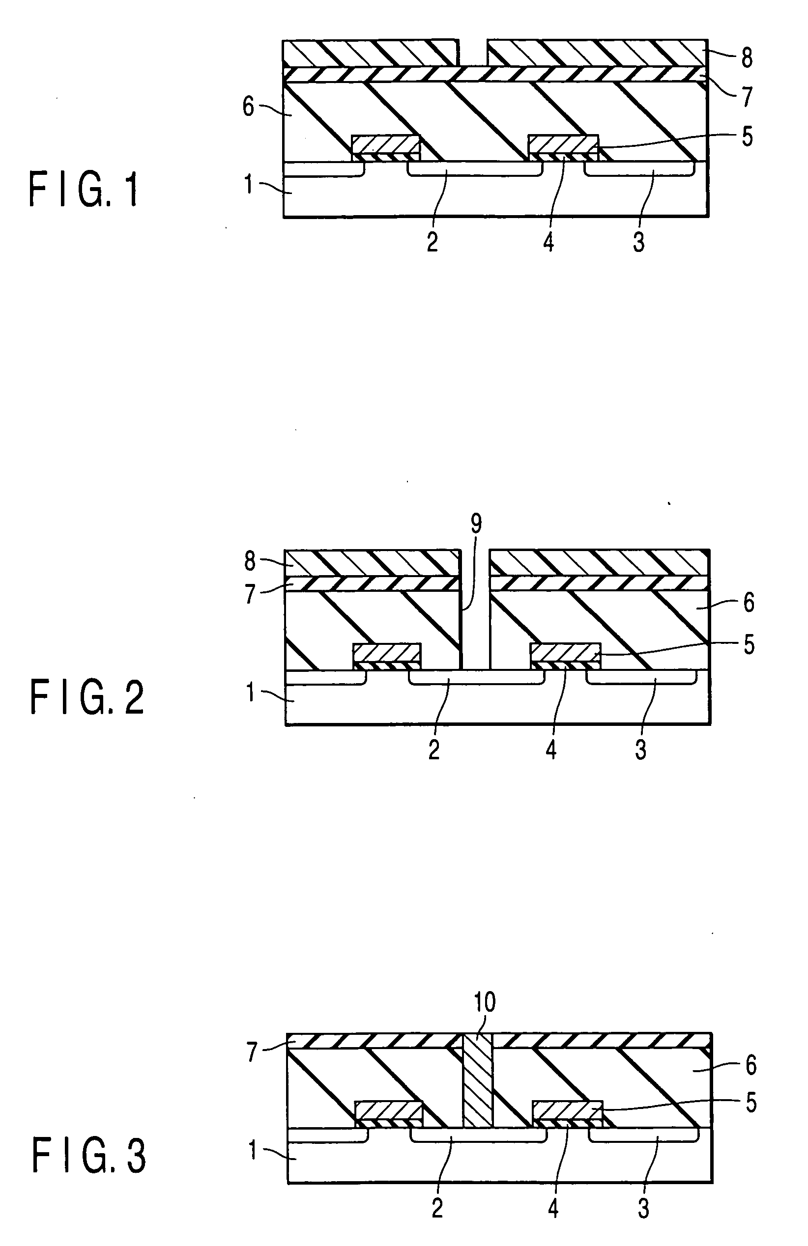
[0049] FIGS. 1 to 8 are cross sectional views collectively showing the process steps included in the manufacturing method of a semiconductor device according to embodiment 1 of the present invention.

[0050] In the first step, an interlayer insulating film 6 and an anti-reflection layer (ARC) 7 that is impermeable to hydrogen are formed successively on a semiconductor substrate 1, followed by forming a resist pattern 8 in direct contact with the ARC 7, as shown in FIG. 1. Formed in the semiconductor substrate 1 is a transistor including a source region 2, a drain region 3, a gate insulating film 4, and a gate electrode 5. It is possible to use, for example, TEOS for forming the interlayer insulating film 6.

[0051] The ARC 7 is required to resist permeation of hydrogen. To be more specific, if the hydrogen diffusion coefficient of a layer at 700° C. is less than 10−11 cm2 / s, the layer can be substantially regarded as resisting permeation of hydrogen. In embodiment 1 of the present inv...

embodiment 2

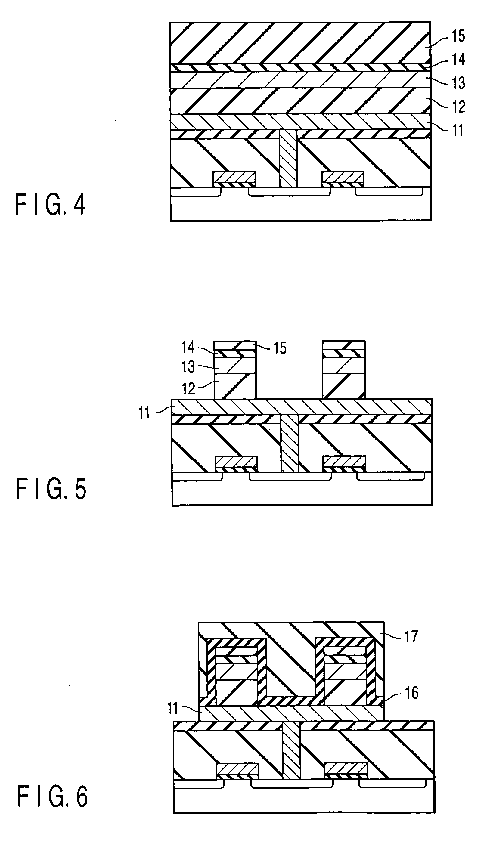
[0060] It is possible to use a conductive material for forming an ARC, which is impermeable to hydrogen and which is formed between the lower electrode of the capacitor and the TEOS film. The particular construction will now be exemplified with reference to FIGS. 9 to 12.

[0061] First of all, the construction shown in FIG. 9 is formed by the method similar to that for embodiment 1 described above, except that the ARC that is impermeable to hydrogen is formed by using a conductive material. The conductive material that can be used for forming the ARC includes, for example, carbon, chromium nitride such as CrN, titanium nitride such as TiN, tantalum nitride such as TaN, aluminum nitride such as AlN, TiAlxNy, TaAlxNy, TiSixNy, AlSixNy (where x and y denote the component ratio), and silicon carbide such as SiC. It is also possible to use silicon oxycarbide such as SiOC, which is a conductive material, for forming the ARC.

[0062] In the next step, the hard mask 15, the hydrogen barrier f...

embodiment 3

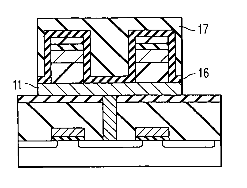
[0065] It is possible to form an ARC that is impermeable to hydrogen on the upper electrode of the capacitor. The particular construction will now be exemplified with reference to FIGS. 13 to 19.

[0066] In the first step, the interlayer insulating film 6, the lower electrode 11, the ferroelectric film 12, the upper electrode 13, the hydrogen barrier film 14 and the hard mask 15 are formed successively on the semiconductor substrate 1 having a transistor formed therein, as shown in FIG. 13. Each of the electrodes and the films noted above can be formed by using the material described previously by a method similar to the method described previously.

[0067] To be more specific, the ARC 7 that is impermeable to hydrogen is formed by using an insulating material on the hard mask 15, followed by forming the resist pattern 8 on the ARC 7. Each of the ARC 7 and the resist pattern 8 can be formed by using the material described previously by a method similar to the method described previous...


PUM


Abstract

Disclosed is a method for manufacturing a semiconductor device, comprising forming an insulating film above a semiconductor substrate having an element formed thereon, forming an anti-reflection layer that is impermeable to hydrogen on the insulating film, the anti-reflection layer comprising a layer formed of at least one material selected from the group consisting of silicon nitride, silicon oxynitride, chromium oxide, CrOxFy, CrAlxOy, AlSixOy, ZrSixOy, silicon oxycarbide, carbon, chromium nitride, titanium nitride, tantalum nitride, aluminum nitride, TiAlxNy, TaAlxNy, TiSixNy, AlSixNy (where x and y denote the component ratio), and silicon carbide, forming a resist pattern on the anti-reflection layer, forming a hole in the insulating film with the resist pattern used as a mask, burying a conductive material in the hole to form a plug, removing the resist pattern, and forming a ferroelectric capacitor above the anti-reflection layer.

Description

CROSS-REFERENCE TO RELATED APPLICATIONS [0001] This application is based upon and claims the benefit of priority from prior Japanese Patent Application No. 2004-171084, filed Jun. 9, 2004, the entire contents of which are incorporated herein by reference. BACKGROUND OF THE INVENTION [0002] 1. Field of the Invention [0003] The present invention relates to a method for manufacturing a semiconductor device, particularly, to a method for manufacturing a semiconductor device including a ferroelectric capacitor. [0004] 2. Description of the Related Art [0005] A ferroelectric material such as lead zirconate titanate (PZT) or strontium bismuth tantalate (SBT) is used for forming a capacitor included in a ferroelectric memory. Such a ferroelectric material is weak against a reducing atmosphere such as a hydrogen atmosphere. If the ferroelectric material noted above is exposed to a hydrogen atmosphere, the oxygen atoms contained in the crystal of the ferroelectric material are extracted, with...

Claims


Application Information

Patent Timeline
IPC IPC(8): H01L21/00H01L21/02H01L27/105H01L21/8242H01L21/8246H01L27/115
CPCH01L27/11502H01L28/65H01L28/57H01L27/11507H10B53/30H10B53/00
Inventor NAKAZAWA, KEISUKEYAMAZAKI, SOICHI
Owner KK TOSHIBA
Why Eureka
Try Eureka