[0010] A further object of the invention is to combine the advantages and best features of the different approaches of the prior art that have not previously been available in a single apparatus, and to do so effectively and efficiently.
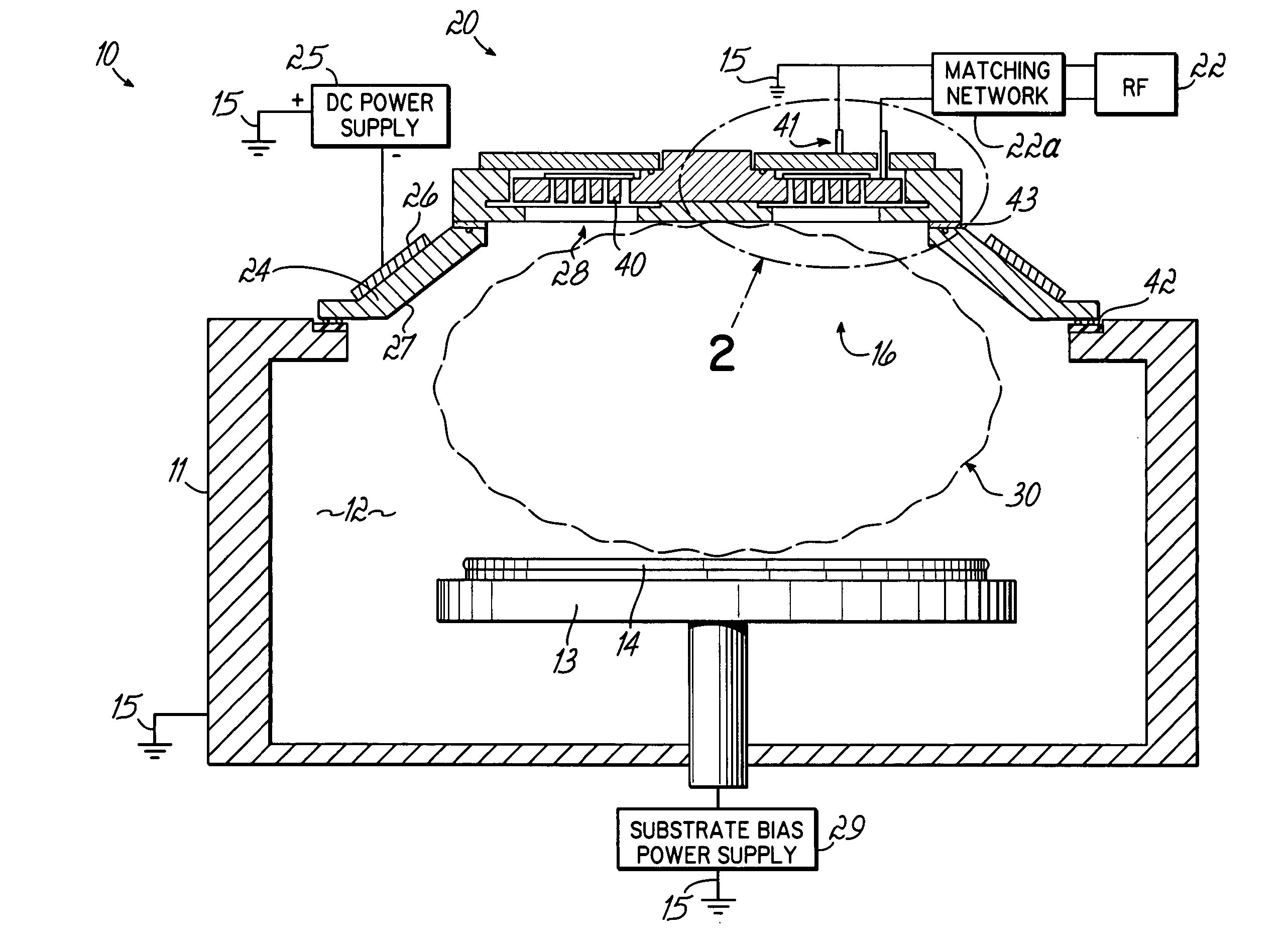
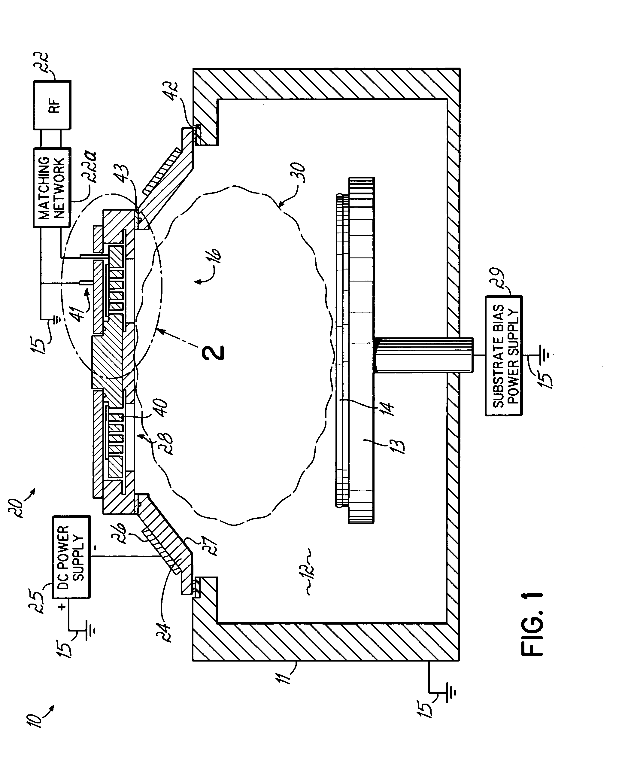
[0012] According to certain embodiments of the invention, a plasma source is provided having one or more of the following features: An internal coil shielded by a plasma shield where the coil and the shield are dimensioned to prevent the ignition of parasitic discharges around the RF coil. An internal coil shielded by a plasma shield where the plasma shield is designed to withstand high temperatures and to absorb most of the plasma
heat load, and thereby eliminate the need to actively cool the RF coil. An internal coil behind which a backplate is provided that is RF and thermally grounded, wherein the backplate may be part of the chamber wall, and alternatively and preferably, is a separate removable component. An internal coil and backplate where the coil cross section is such that it reduces
metal deposition on the backplate behind the coil. An internal coil where the shape of the RF coil is preserved by stiffeners mounted on the side facing the backplate. Coil stiffeners supporting a coil and including several radial stiffening members made of
dielectric material that may be attached to the coil, preferably out of contact with the backplate. Coil stiffeners profiled, on the side facing the plasma, to prevent the formation of a conducting path of deposited material from one turn of the coil to the another. A coil and backplate
assembly in which the backplate has grooves machined at locations corresponding to coil stiffening members, to preserve the design spacing of the backplate, preferably of 2 mm or less, from the coil. A coil and plasma shield wherein the shield is configured to absorb most of the plasma
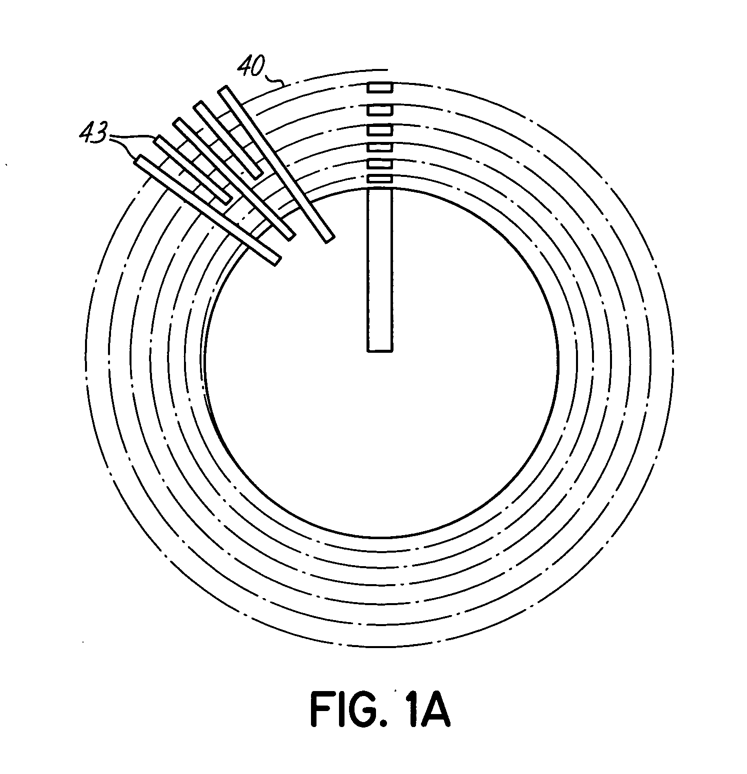
heat load and allow a non-negligible fraction of metal flux to deposit on the coil, which simplifies the profile of the shield and increases its RF transparency. Such a shield having several the radial slots for
RF transmission. A vacuum seal for the coil RF feed. A coil and backplate
assembly in which the center of the coil is thermally and electrically grounded to the backplate. A coil and backplate
assembly having an RF feed connected to the outer part of the coil and vacuum seals against the backplate with a two-part sealing assembly.
[0013] There are several advantages of the features of the invention that accomplish the objectives of the invention and improve upon the prior art. The backplate can sustain a substantially larger amount of
metal deposition than the
dielectric window in the external coil configuration. Coil stiffeners keep the coil from sagging and coming into contact with the plasma shield. The backplate supports most of the
atmospheric pressure against the vacuum. The advantages of this invention over other iPVD sources include a less restrictive requirement on metal flux shielding. The shield shields the coil from the plasma heat load. Some metal is allowed to pass through the shield and deposit on the coil, allowing a thinner shield with less complicated slots, and good RF transparency. The coil need not be actively cooled, is not sputtered, and is thus not consumable, but may be cleaned from
metal deposition from time to time. Since the coil is enclosed in a small conductive space, its
inductance is about 50% less than in typical iPVD sources, resulting in reduced coil
voltage, which can be exploited in two ways: 1) by simplifying some of the constraints on the design and construction of the tuning network and RF connectors, or 2) by at least partially trading off the reduced coil
voltage for a reduced coil current, for example, by increasing the number of coil turns and thereby reducing the current through the coil. Such a source coil has a much lower profile than a three-dimensional ICP coil.
[0015] Depending on the application, some of the features may be more or less important. In exclusively low-pressure applications, the requirements on the spacing of the backplate from the coil can be larger than 2 mm. Also, if the plasma heat load or
sputtering is not excessive, as for example for operations in the range of several hundred watts, the plasma shield may be omitted. At the opposite extreme, for very
high density plasmas,
active cooling of the coil and plasma shield may be necessary. Also, depending on applications, the level of metal deposition on the
ground plane and stiffeners may be unacceptable. In that case, the coil cross section may be changed from a rectangular shape to a chevron shape, so that the coil conductors themselves block
line of sight paths through the coil. While more complex, this configuration will substantially reduce the level of metal deposition behind the coil
[0016] In etch applications, the present invention results in a uniform, high etch rate at a reduced voltage. Other applications of the invention allow a pre-clean step to be performed in situ in an IPVD module.

