Thin film magnetic memory device and semiconductor integrated circuit device including the same as one of circuit blocks

a magnetic memory and integrated circuit technology, applied in semiconductor devices, digital storage, instruments, etc., can solve the problems of non-uniform thickness of finished straps, non-uniform thickness of films, and difficulty in uniform manufacturing of mtj memory cells within memory cell arrays, so as to achieve efficient magnetization, suppress erroneous data writes due to magnetic noise, and uniform dimensions, shapes and structures of magnetic memory cells

Inactive Publication Date: 2006-01-05
RENESAS ELECTRONICS CORP
View PDF5 Cites 15 Cited by
  • Summary
  • Abstract
  • Description
  • Claims
  • Application Information

AI Technical Summary

Benefits of technology

[0053] Accordingly, a main advantage of the present invention is that variation in the density, being high or low, of magnetic memory cells between areas in the center portion and in border portions of the memory cell array can be eliminated by arranging shape dummy cells in the peripheral portion of the memory cell array in a thin film magnetic memory device. As a result, the uniformity of the dimensions, shapes and structures of the magnetic memory cells can be attained within the memory cell array.
[0054] A semiconductor integrated circuit device according to another configuration of the present invention includes a plurality of circuit blocks, wherein each circuit block includes a magnetic memory cell array in which a plurality of magnetic memory cells is arranged. Each magnetic memory cell has a magnetic memory element having a plurality of magnetic layers at least one of which is magnetized in the direction in accordance with storage data, and the plurality of magnetic memory cells is arranged so that the easy axis of the magnetic memory element in each magnetic memory cell is oriented in the same direction relative to the plurality of circuit blocks.
[0055] The direction (easy axis) in which magnetic memory cells are arranged is oriented in the same direction relative to the plurality of circuit blocks in such a semiconductor integrated circuit device and, therefore, the respective magnetic memory cells can be collectively and efficiently magnetized in the magnetization process of the magnetic memory cells, which is inevitably included in the manufacturing process of the semiconductor integrated circuit device.
[0056] A thin film magnetic memory device according to another configuration of the present invention includes a memory cell array in which a plurality of magnetic memory cells are sequentially arranged, wherein each memory cell includes a magnetic memory element having a plurality of magnetic layers at least one of which is magnetized in the direction in accordance with storage data. The thin film magnetic memory device further includes a data write wire that allows a data write current to pass through the data write wire so as to generate a data write magnetic field applied to the magnetic memory elements and with a plurality of wires in addition to the data write wire, wherein the data write wire and the plurality of wires are arranged in a layout that the sum of magnetic fields generated by currents passing through the plurality of wires, respectively, becomes smaller than a predetermined magnetic field.
[0057] Accordingly, the arrangement of these wires is determined by taking into consideration the amount of magnetic noise from wires other than the group of wires which directly affect the magnetic memory cells and, therefore, erroneous data write due to magnetic noise can be suppressed.

Problems solved by technology

A problem arises wherein uniform manufacture of MTJ memory cells within a memory cell array becomes difficult because areas of high and low density occur when a plurality of MTJ memory cells is arranged in the same chip.
As a result of this, non-uniformity occurs in the thickness of the finished strap SRP.
This is caused by the non-uniformity in the film thickness of strap SRP occurring in step (a).
At the time of over etching, however, strap SRP, which has been formed as a thin layer, is further shaved in the low density region of the pattern and, in some cases, there is a possibility that strap SRP pattern may disappear.
As a result of this, non-uniformity in the planar memory cell form occurs between the high density region of the pattern and the low density region of the pattern in the above described manner.
There is a risk, however, wherein buffer layer 430 in an MTJ memory cell in the high density region of the pattern may be excessively shaved due to the effects of a step that occurs between the high density region of the pattern and the low density region of the pattern at the time of polishing of buffer layer 430 in the planarization process.
Thereby, there is a danger of defective electrical coupling (fluctuation in electric resistance) between tunneling magneto-resistance element TMR and bit line BL as well as a danger of negative effects to the magnetic layers of which tunneling magneto-resistance element TMR is formed.
As described above, in the case where a region having a high density of MTJ memory cells and region having a low density of MTJ memory cells exist in a mixed manner within the same chip, a certain degree of non-uniformity in the forms and dimensions of MTJ memory cells inevitably occurs between these regions.
Accordingly, there is a risk wherein erroneous data write may take position due to the occurrence of magnetic noise in a memory cell other than the selected memory cell that has been selected as the object of data write.
In particular, there is a high risk of erroneous data write to a group of non-selected memory cells belonging to the same row or the same column as the selected memory cell due to an overlap of magnetic noise because either the easy axis (EA) or the hard axis (HA) of this group of non-selected memory cells is subject to a data write magnetic field of a predetermined intensity.

Method used


Image

  • Thin film magnetic memory device and semiconductor integrated circuit device including the same as one of circuit blocks
  • Thin film magnetic memory device and semiconductor integrated circuit device including the same as one of circuit blocks
  • Thin film magnetic memory device and semiconductor integrated circuit device including the same as one of circuit blocks

Examples


first embodiment

[0101] A configuration for ensuring the uniformity of the memory cell pattern (memory cell dimensions, forms and structures) within a memory array wherein MTJ memory cells for data storage are arranged is described in a first embodiment.

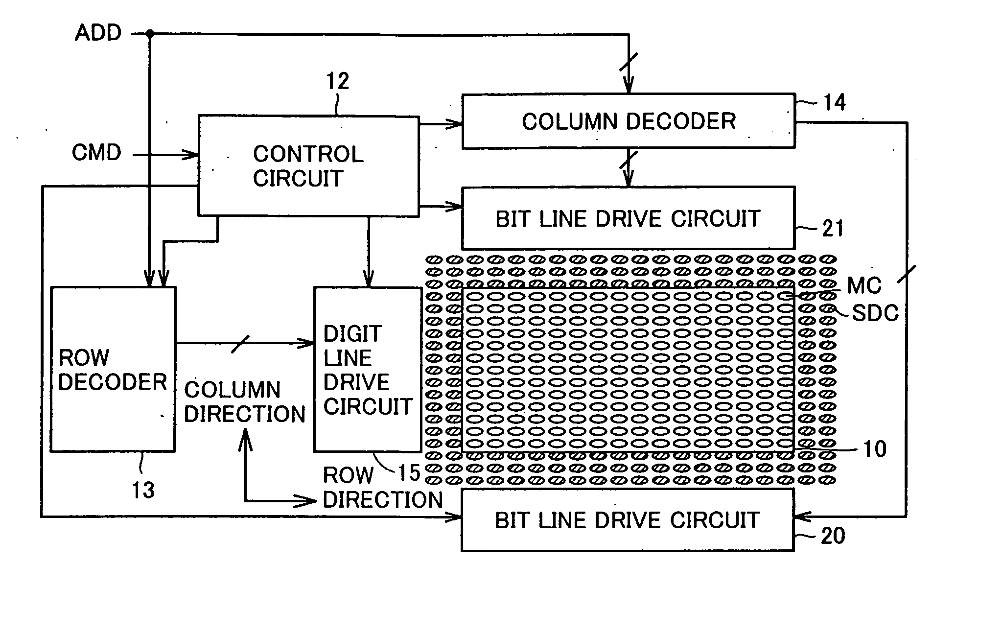
[0102] With reference to FIG. 1, an MRAM device according to the embodiment of the present invention is provided with an MTJ memory cell array 10 wherein MTJ memory cells MC for data storage are arranged in sequence in a matrix. Here, in the following, MTJ memory cells arranged within MTJ memory cell array 10 that becomes an access object in accordance with an address signal ADD is specifically referred to as “normal memory cells” in order to be distinguished from the shape dummy cells described below in the present specification.

[0103] The MRAM device is further provided with a control circuit 12 for controlling the entire operation of the MRAM device in response to a control signal CMD, a row decoder 13 for carrying out a row selection of the nor...

first modification

of First Embodiment

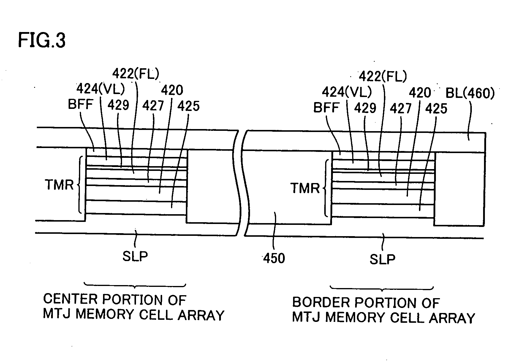
[0135] Though a case is shown in the first embodiment wherein shape dummy cells SDC are used in an MTJ memory cell array having a general configuration, as shown in FIGS. 1 and 3, shape dummy cells SDC can be used in the same manner in other memory cell array configurations.

[0136] With reference to FIG. 6, a plurality of MTJ memory cells MC (tunneling magneto-resistance elements TMR) arranged in a matrix in MTJ memory cell array 10 is divided into a plurality of row blocks RB(1) to RB(M) (M: integer of 2, or greater) in the row direction in a first modification of the first embodiment. Each of row blocks RB(1) to RB(M) has L memory cell rows (L: integer of at least 2). FIG. 2 shows an example having a configuration wherein L=4. Here, in the following, row blocks RB(1) to RB(M) are generically and simply referred to as row blocks RB.

[0137] Straps SRP arranged as signal lines in the column direction are provided so as to correspond to row blocks RB(1) to RB(M), re...

second modification

of First Embodiment

[0152] An example of the layout of shape dummy cells in the case where the MTJ memory cell array is broken down into a plurality of blocks is shown in a second modification of the first embodiment.

[0153] With reference to FIG. 8, MTJ memory cell array 10 is arranged so as to be divided into a plurality of memory blocks 11 in the second modification of the first embodiment. Normal memory cells MC are arranged in a matrix in each memory block 11. Correspondingly, digit line drive circuits 15 and bit line drive circuits 20 and 21 are arranged so as to be divided to correspond to memory blocks 11, respectively. Here, the configuration of the MTJ memory cell array is not specifically limited and the configurations shown in FIG. 4 and in FIG. 7 can be used.

[0154] Shape dummy cells SDC are arranged so as to be in sequence with normal memory cells MC in the row direction and in the column direction in respective memory blocks 11 in the configuration the second modificat...


PUM


Abstract

Shape dummy cells that are designed to have the same dimensions and structures as MTJ memory cells are additionally provided in the peripheral portion of an MTJ memory cell array in which normal MTJ memory cells for storing data are arranged in a matrix. The MTJ memory cells and the shape dummy cells are sequentially arranged so as to have a uniform pitch throughout the entirety. Accordingly, non-uniformity between MTJ memory cells in the center portion and in border portions of the MTJ memory cell array, respectively, after manufacture due to high and low densities of the surrounding memory cells can be eliminated.

Description

BACKGROUND OF THE INVENTION [0001] 1. Field of the Invention [0002] The present invention relates to a thin film magnetic memory device, and more particularly to a thin film magnetic memory device provided with a memory cell having a magnetic tunnel junction (MTJ) and a semiconductor integrated circuit device including the thin film magnetic memory device as one of circuit blocks. [0003] 2. Description of the Background Art [0004] MRAM (Magnetic Random Access Memory) devices have obtained attention as memory devices that can store nonvolatile data while consuming low power. An MRAM device is a memory device using a plurality of thin film magnetic materials formed in a semiconductor integrated circuit for storing nonvolatile data and for allowing random access to the respective thin film magnetic materials. [0005] In particular, rapid progress in the performance of MRAM devices due to the use of a thin film magnetic material, wherein a magnetic tunnel junction is utilized, as a memor...

Claims


Application Information

Patent Timeline
Patent Type & Authority Applications(United States)
IPC IPC(8): G11C7/02G11C11/16H01L27/105H01L21/8246H01L43/08
CPCB82Y10/00H01L27/228G11C11/16G11C11/1659G11C11/1657G11C11/1675H10B61/22
Inventor OOISHI, TSUKASA
Owner RENESAS ELECTRONICS CORP
Why Eureka
Try Eureka