Semiconductor device substrate with embedded capacitor

a technology of semiconductor devices and capacitors, applied in semiconductor devices, capacitors, electrical equipment, etc., can solve the problems of inefficient use of active device area space, difficult formation of trenches and electrode materials,

Inactive Publication Date: 2006-01-05
TAIWAN SEMICON MFG CO LTD
View PDF6 Cites 16 Cited by
  • Summary
  • Abstract
  • Description
  • Claims
  • Application Information

AI Technical Summary

Problems solved by technology

One challenge for increasing DRAM density is maintain the same cell capacitance as memory cell sizes are scaled down.
As DRAM memory cell sizes decrease, the formation of trenches and electrode materials is increasingly difficult due to small etching process windows and the difficulty in handling advanced electrode and capacitor dielectric materials.
Another problem with prior art approaches to producing DRAM devices is the inefficient use of active device area space, for example, in the substrate underlying the MOS transistor source and channel regions, frequently increasing the DRAM cell area by forming capacitors adjacent the bit and word lines and / or taking part of the drain area.

Method used


Image

  • Semiconductor device substrate with embedded capacitor
  • Semiconductor device substrate with embedded capacitor
  • Semiconductor device substrate with embedded capacitor

Examples


Embodiment Construction

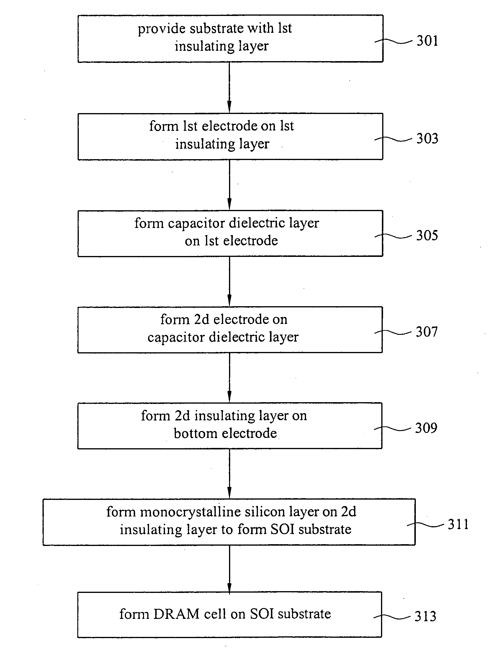
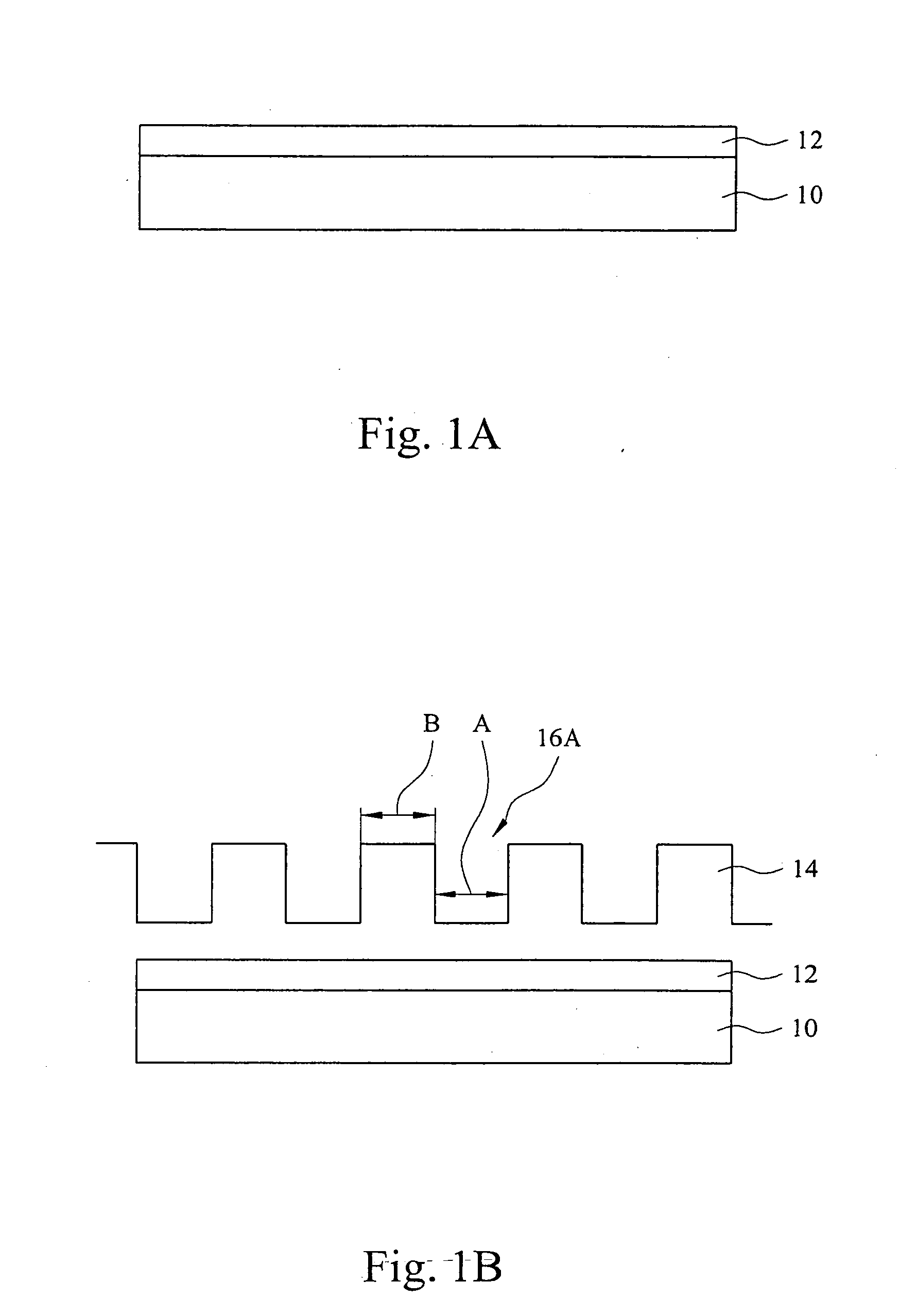
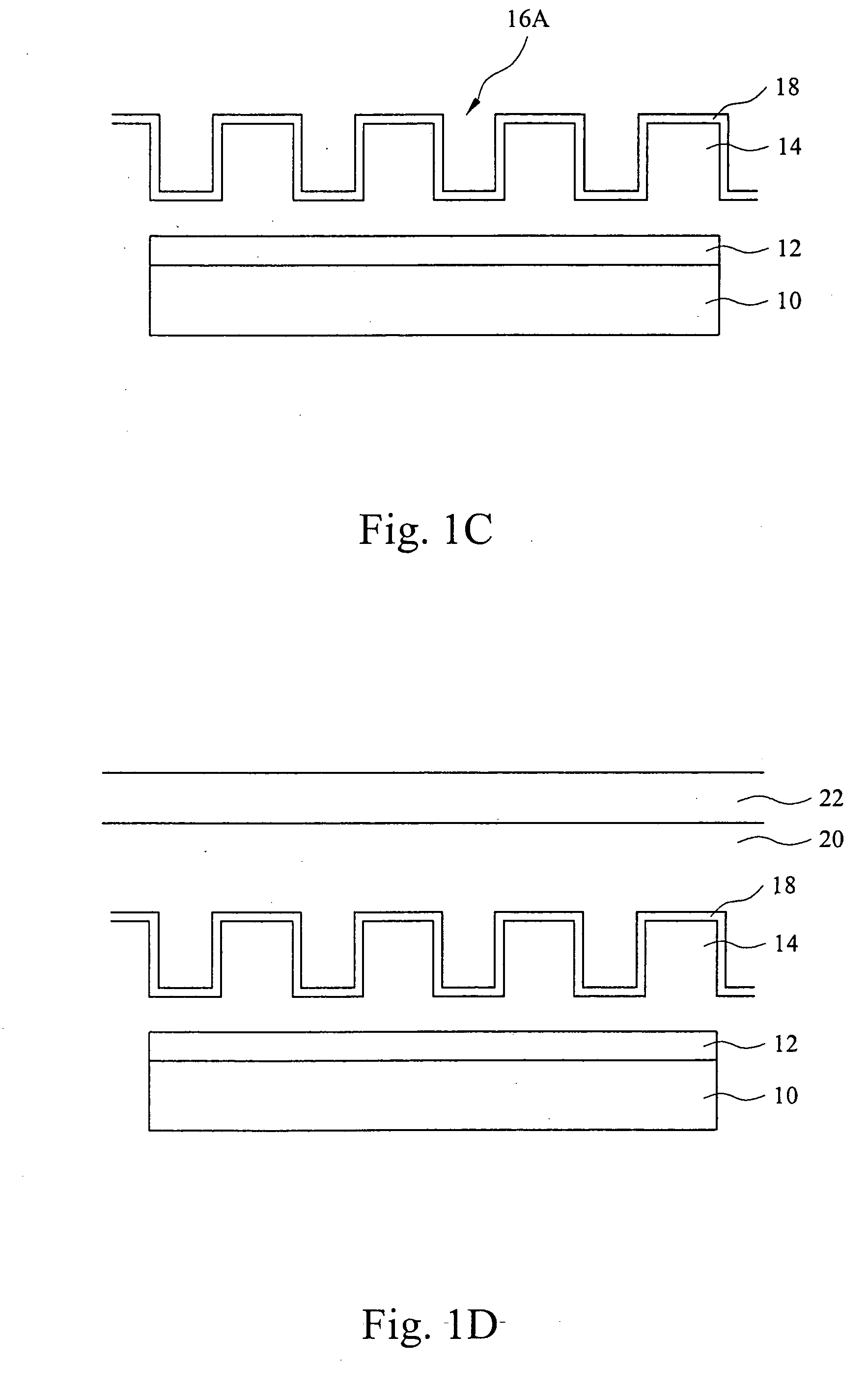
[0016] Referring to FIG. 1A, is shown a substrate 10, for example a semiconductor wafer such as silicon. An electrically insulating layer 12, for example an oxide such as silicon oxide is grown and / or deposited over the substrate 10 by conventional processes to a predetermined thickness.

[0017] Referring to FIG. 1B, an electrically conductive material layer 14 is the formed over the electrically insulating layer 12 at a desired thickness to form a first capacitor electrode layer to a desired thickness. The first capacitor electrode layer may formed of any electrically conductive material including metals, metal oxides, metal nitrides, and metal oxynitrides as well as semiconductor materials such as doped or undoped polysilicon. The first capacitor electrode layer 14 is then patterned by conventional methods e.g., photoresist and / or a nitride hardmask, followed by a wet or dry etching process to form a series of spaced trench openings e.g., 16A through a thickness portion of the elec...


PUM


Abstract

A method for forming a semiconductor device including a DRAM cell structure comprising a silicon on insulator (SOI) substrate with an embedded capacitor structure including providing a substrate comprising an overlying first electrically insulating layer; forming a first electrically conductive layer on the first electrically insulating layer to form a first electrode; forming a capacitor dielectric layer on the first electrode; forming a second electrically conductive layer on the capacitor dielectric layer to form a second electrode; forming a second electrically insulating layer on the second electrode; and, forming a monocrystalline silicon layer over the second electrode to form an SOI substrate comprising a first capacitor structure.

Description

FIELD OF THE INVENTION [0001] This invention generally relates to microelectronic integrated circuit (IC) semiconductor device fabrication and more particularly to DRAM devices including a substrate with an embedded capacitor. BACKGROUND OF THE INVENTION [0002] Dynamic random access memory (DRAM) is a staple aspect of the main memory of PC systems. DRAM may be used as an embedded portion of an integrated circuit or be formed as an array of memory cells. Fir example, in memory cell arrays an MOS transistor and a capacitor make up a memory unit (cell) whereby word-lines are used to switch a pass transistor between an on and of state to connect the bit line to the capacitor or to isolate the capacitor. The bit line is used for both the read and write operations to the storage node of the capacitor. [0003] Generally, three types of DRAM memory cells are in use including planar capacitor DRAM cells, stack capacitor DRAM cells and trench capacitor DRAM cells. A key element of DRAM devices...

Claims


Application Information

Patent Timeline
Patent Type & Authority Applications(United States)
IPC IPC(8): H01L21/8234H01L21/8244H01L21/8242
CPCH01L21/8221H01L21/84H01L27/0688H01L27/10832H01L28/82H01L27/10858H01L27/10861H01L27/1203H01L28/55H01L27/10835H10B12/373H10B12/377H10B12/036H10B12/038
Inventor LIN, CHUN-CHIEHLEE, WEN-CHIN
Owner TAIWAN SEMICON MFG CO LTD
Why Eureka
Try Eureka