Method for fabricating semiconductor device

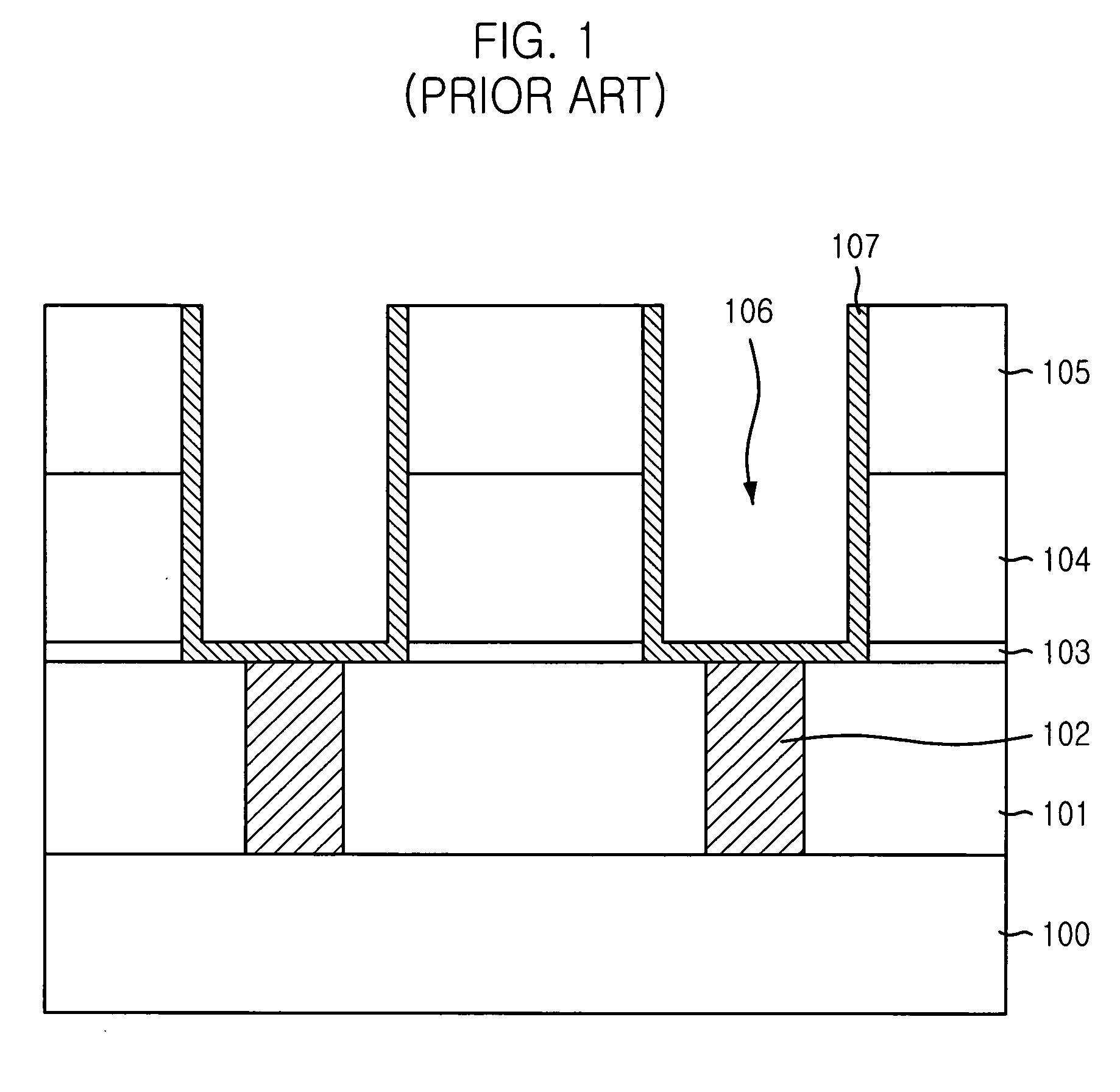
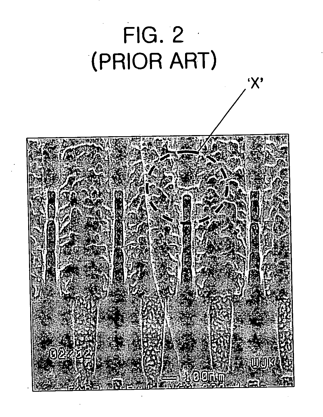
a semiconductor and device technology, applied in the direction of semiconductor devices, capacitors, electrical equipment, etc., can solve the problems of difficult to obtain the critical dimension (cd) at the bottom portion of the opening, the psg layer 104/b> is more easily damaged, and the capacitor oxide structure is created. , to achieve the effect of preventing bridge formation and reducing the density of the psg layer

Active Publication Date: 2006-01-05
CONVERSANT INTPROP MANAGEMENT INC
View PDF12 Cites 20 Cited by
  • Summary
  • Abstract
  • Description
  • Claims
  • Application Information

AI Technical Summary

Benefits of technology

[0027] It is, therefore, an object of the present invention to provide a method for fabricating a semiconductor device capable of preventing bridge formation between isolated conductive layers caused by the fact that a stack oxide structure including a tetraethylorthosilicate (

Problems solved by technology

However, as the TEOS layer is thickly deposited with a thickness of 20,000 Å for the purpose of increasing the capacitance, an aspect ratio increases in the etching process for forming the openings that exposes the storage node contact plugs, and as a result, it is difficult to obtain a desired critical dimension (CD) at a bottom portion of the opening.
However, during the wet cleaning process, the capacitor oxide structure, i.e., the TEOS layer 105 and the PSG layer 104, is damaged, resulting in creation of a tunnel in the capacitor oxide structure.
As a result, the PSG layer 104 is more easily damaged during the wet cleaning process, thereby creating the tunnel.
Thus, during the wet cleaning process, the interface between the PSG layer 104 and the TEOS layer 105 is damaged as the cleaning solution flows through the interface, thereby creating the tunnel.
A reference denota

Method used


Image

  • Method for fabricating semiconductor device
  • Method for fabricating semiconductor device
  • Method for fabricating semiconductor device

Examples


first embodiment

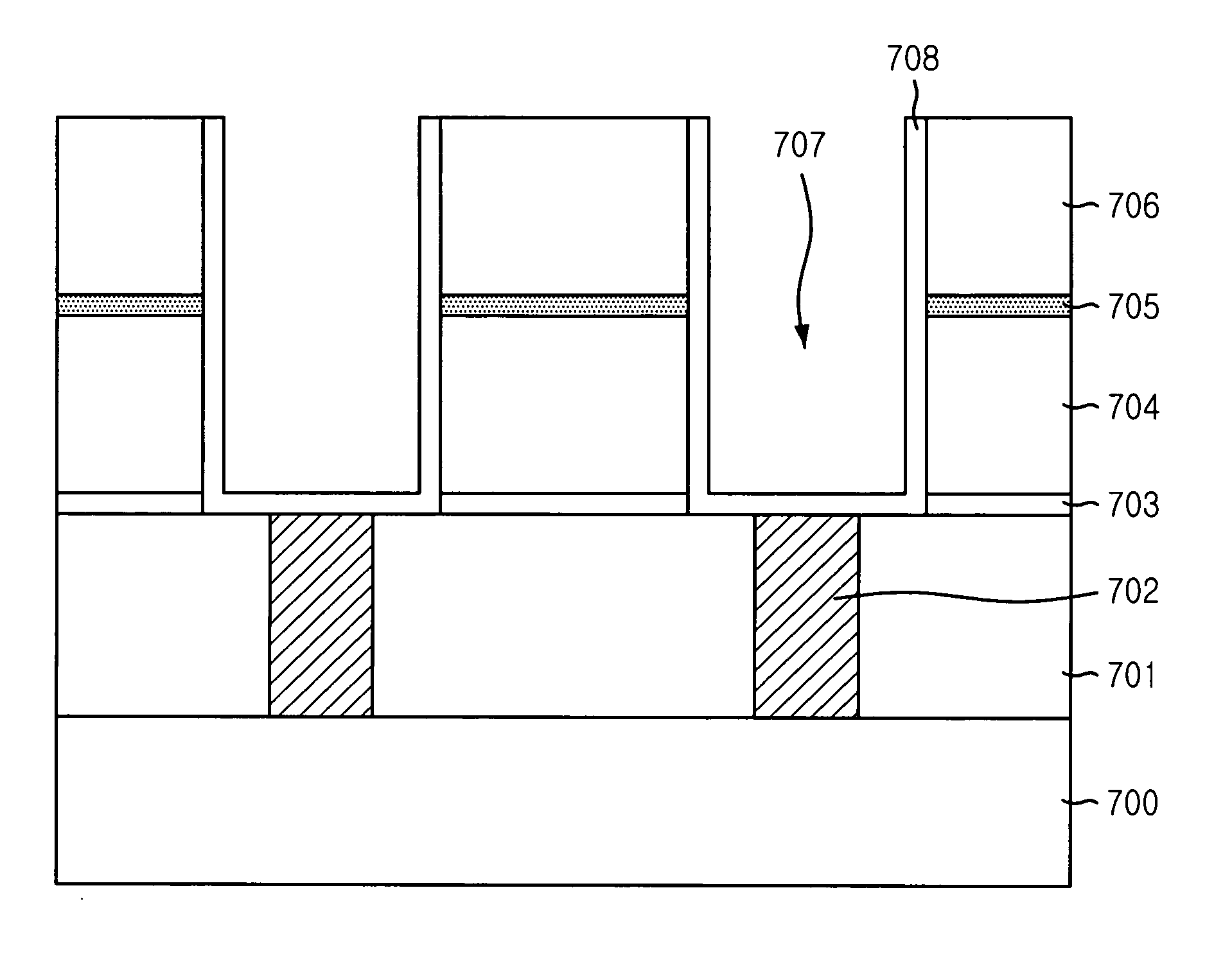
[0048]FIG. 6 is a flowchart for showing sequential steps of a method for fabricating a semiconductor device in accordance with the present invention.

[0049] As shown in the flowchart, at step S601, a phosphosilicate glass (PSG) layer is formed on a substrate provided with various device elements. Herein, the substrate includes conductive regions which can be gate electrodes, bit lines, metal wires, contact plugs, and contact pads.

[0050] At step S602, a capping layer for preventing an incidence of phosphorus diffusion from the PSG layer to a subsequent tetraethylorthosilicate (TEOS) layer caused by a difference in a phosphorus concentration gradient between the PSG layer and the TEOS layer. At this time, a thickness of the capping layer is approximately 1 / 19 to approximately 1 / 9 of that of the PSG layer. That is, the capping layer has a thickness ranging from approximately 100 Å to approximately 500 Å. Also, the capping layer is made of a material selected from a group consisting of ...

second embodiment

[0074]FIG. 8 is a flowchart showing sequential steps of a method for fabricating a semiconductor device in accordance with the present invention.

[0075] At step S801, a PSG layer is formed on a substrate provided with various device elements. Herein, the substrate includes conductive regions which can be gate electrodes, bit lines, metal wires, contact plugs, and contact pads.

[0076] At step S802, a surface of the PSG layer is scrubbed in order to make the PSG layer exhibiting hydrophobicity when a subsequent process is delayed by more than a predetermined period, e.g., approximately 5 hours, hydrophilic. The scrubbing proceeds by employing a rinsing process with use of pure water for approximately 40 seconds to approximately 80 seconds. It is also possible to perform the rinsing process in vibration by using pure water for approximately 10 seconds to approximately 30 seconds.

[0077] Meanwhile, since the PSG layer is doped with a high concentration of phosphorus, the surface of the P...

third embodiment

[0122] In accordance with the present invention, adhesiveness between the PSG layer and the TEOS layer can be improved by forming the TEOS layer on the stabilized PSG layer obtained through the application of the plasma treatment. As a result of this improved adhesiveness, it is possible to prevent damages to the interface between the PSG layer and the TEOS layer during the wet cleaning process for removing the etch remnants and the interfacial oxide layer at each bottom surface of the openings.

[0123] In accordance with the first to the third embodiments of the present invention, for the case of the tunnel formation during the wet cleaning process because of a decrease in the density of the PSG layer as phosphorus contained in the PSG layer diffuses from the PSG layer to the TEOS layer and because of a degraded interface characteristic between the PSG layer and the TEOS layer caused by the diffused phosphorus reacting with moisture of the atmosphere, the capping layer is formed on t...


PUM


Abstract

The present invention relates to a method for fabricating a semiconductor device capable of preventing bridge formation caused by damages to a capacitor oxide structure including a phosphosilicate glass (PSG) layer and a tetraethylorthosilicate (TEOS) layer during a wet cleaning process. The method includes the steps of: forming a PSG layer on a substrate; forming a capping layer on the PSG layer; forming a TEOS layer on the capping layer; selectively etching the TEOS layer, the capping layer and the PSG layer to form a plurality of openings exposing predetermined portions of the substrate; cleaning the openings; forming a conductive layer on the openings; and removing the conductive layer until the TEOS layer is exposed, so that the conductive layer is isolated for each opening.

Description

FIELD OF THE INVENTION [0001] The present invention relates to a method for fabricating a semiconductor device; and more particularly, to a method for fabricating a semiconductor device capable of preventing generation of bridges between conductive structures caused by damaged insulation layer during a wet cleaning process. DESCRIPTION OF RELATED ARTS [0002] As the scale of integration of a semiconductor device has been advanced, there have been various attempts to secure a sufficient capacitance as much as the decreased pitch between device elements. One of the attempts is to increase a height of a capacitor and form the capacitor in a cylinder or concave type. [0003]FIG. 1 is a cross-sectional view of a semiconductor device in which storage nodes are formed. [0004] As shown, an insulation layer 101 is formed on a substrate provided with transistors, wells and bit lines. Although not illustrated, conductive regions are formed on predetermined portions of the substrate 100. There ar...

Claims


Application Information

Patent Timeline
IPC IPC(8): H01L21/469H01L21/02H01L21/3105H01L21/8242H01L21/768
CPCH01L21/3105H01L21/76801H01L21/76814H01L28/91H01L21/76826H01L21/76829H01L27/10852H01L21/76822H10B12/033H10B99/00
Inventor ROH, JAI-SUN
Owner CONVERSANT INTPROP MANAGEMENT INC
Why Eureka
Try Eureka