Display device and method for production thereof
- Summary
- Abstract
- Description
- Claims
- Application Information
AI Technical Summary
Benefits of technology
Problems solved by technology
Method used
Image
Examples
examples
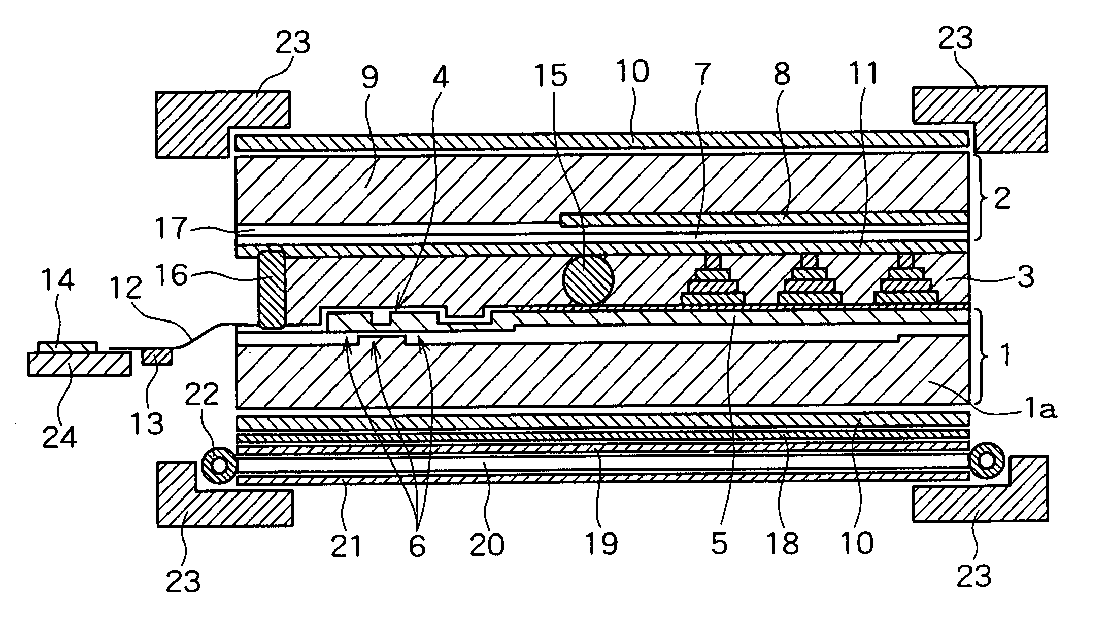
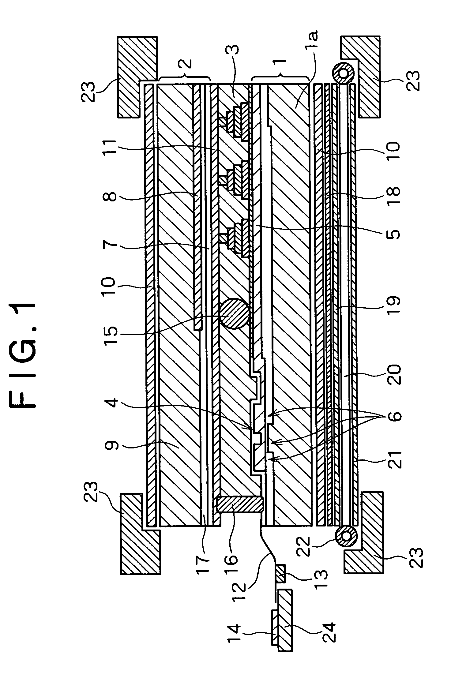
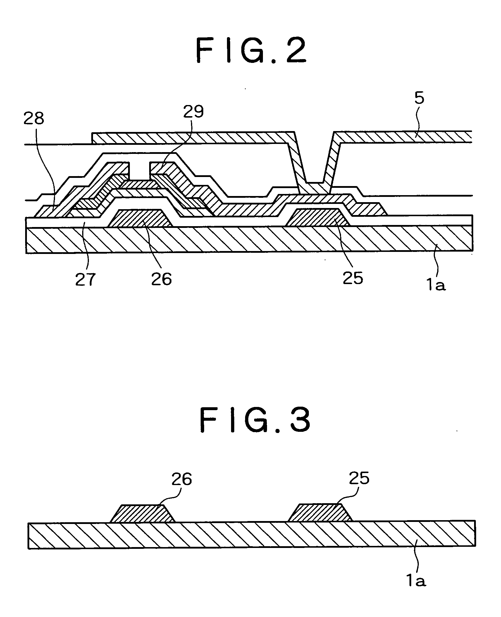
[0134] Table 1 shows the results of measurements of contact resistance between the transparent conductive film 5 (on the substrate with TFT array) and the aluminum alloy film, which are in direct contact with each other.
[0135] The experiments for measurements were carried in the following manner. (1) Constitution of transparent conductive film: Indium tin oxide (ITO) composed of indium oxide and 10 wt % of tin oxide; or indium zinc oxide (IZO) composed of indium oxide and 10 wt % of zinc oxide. The film thickness is 200 nm in both cases. (2) Constitution of aluminum alloy film: Aluminum alloy containing 2 atom % of Ni; or aluminum alloy containing 2 atom % of Ni and 0.6 atom % of Nd. (3) Formation of transparent conductive film:
Condition A in the Initial Stage of Formation.
[0136] Atmosphere gas: argon
[0137] Pressure: 3 mTorr
[0138] Sputter power density: 1.9 W / cm2
[0139] Film thickness: 20 nm
Condition B in the Later Stage of Formation:
[0140] Atmosphere gas: argon / oxygen mixe...
PUM
 Abstract
Description
Claims
Application Information
 - Generate Ideas
- Intellectual Property
- Life Sciences
- Materials
- Tech Scout
- Unparalleled Data Quality
- Higher Quality Content
- 60% Fewer Hallucinations
Browse by: Latest US Patents, China's latest patents, Technical Efficacy Thesaurus, Application Domain, Technology Topic, Popular Technical Reports.
© 2025 PatSnap. All rights reserved.Legal|Privacy policy|Modern Slavery Act Transparency Statement|Sitemap|About US| Contact US: help@patsnap.com


