Method of manufacturing a semiconductor device and semiconductor manufacturing apparatus

a manufacturing apparatus and semiconductor technology, applied in the direction of semiconductor devices, electrical devices, transistors, etc., can solve the problems of productivity and throughput, productivity and throughput are greatly reduced, etc., to reduce impurity contamination, improve electrical characteristics, and suppress the dispersion of tfts electrical characteristics.

Inactive Publication Date: 2006-01-12
SEMICON ENERGY LAB CO LTD +1
View PDF45 Cites 3 Cited by
  • Summary
  • Abstract
  • Description
  • Claims
  • Application Information

AI Technical Summary

Benefits of technology

[0022] The present invention has been made in view of the above-mentioned problems and an object of the present invention is to suppress dispersion in the electrical characteristics of TFTs manufactured based on semiconductor films, and to improve their electrical characteristics, by removing a natural oxide film that is a cause of contamination and dispersion during laser annealing, and by reducing impurity contamination of the semiconductor film surface which is susceptible to contamination.

Problems solved by technology

With this method, however, the atmosphere used for laser annealing must be changed between the first laser anneal and the second laser anneal, which is a problem for productivity and throughput.
Further, it is necessary to perform laser annealing preprocessing and laser annealing by using separate apparatuses at present, and performing processing by using a plurality of apparatus leads to a problem in that productivity and throughput are greatly reduced.

Method used


Image

  • Method of manufacturing a semiconductor device and semiconductor manufacturing apparatus
  • Method of manufacturing a semiconductor device and semiconductor manufacturing apparatus
  • Method of manufacturing a semiconductor device and semiconductor manufacturing apparatus

Examples


embodiment mode 1

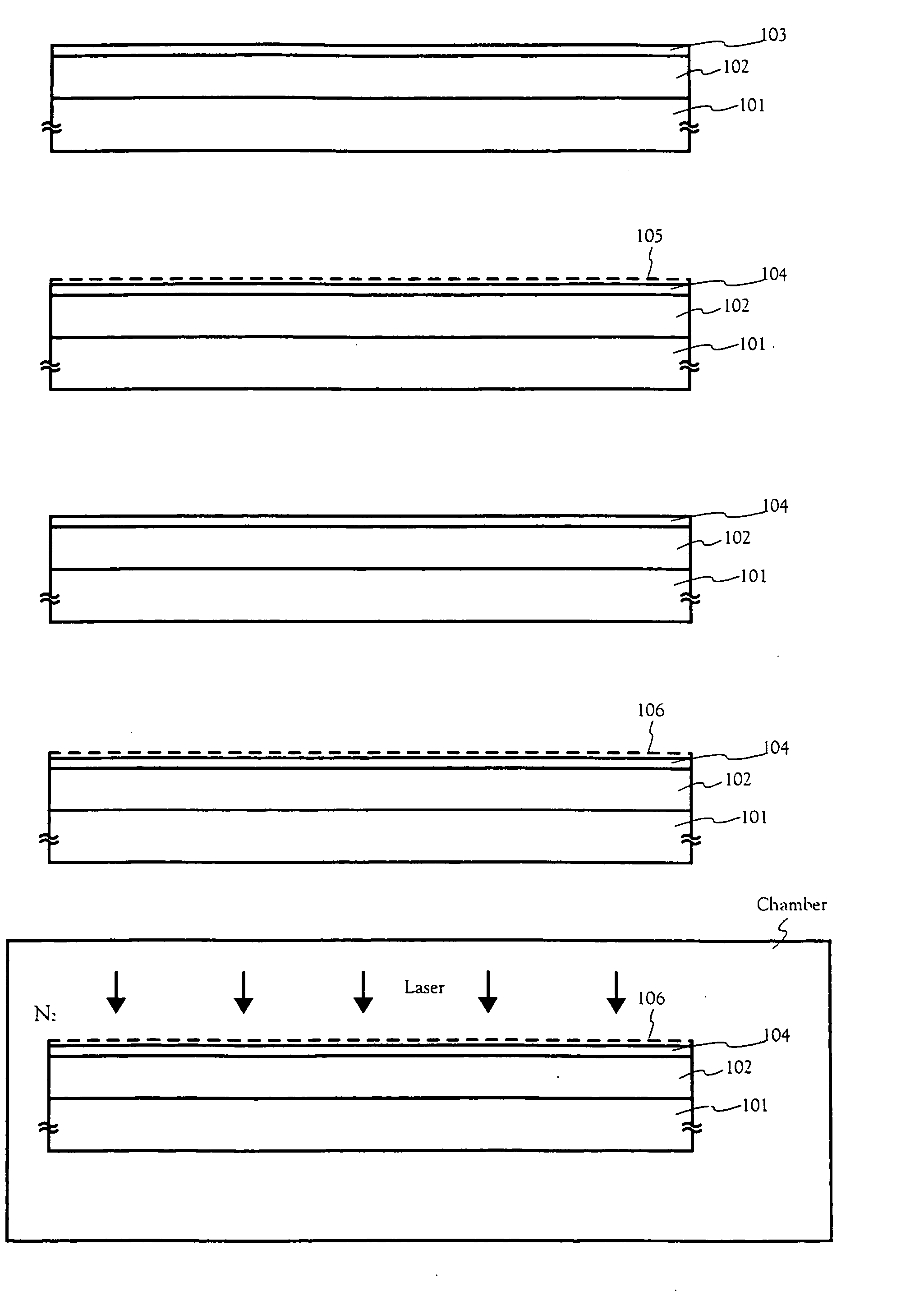
[0087] An explanation is given using FIGS. 2A to 2E for a method of manufacturing a crystalline semiconductor film having reduced impurity contamination. A natural oxide film is removed, an oxidation process is performed, and laser annealing is performed when implementing laser annealing after introducing a metallic element into an amorphous semiconductor film and performing heat treatment. Note that the amorphous semiconductor film is an amorphous silicon film, and that the crystalline semiconductor film is a crystalline silicon film.

[0088] A base insulating film 102 is formed first on a substrate 101. An insulating film such as a silicon oxide film, a silicon nitride film, or a silicon oxynitride film is formed as the base film 102. An example of using a single layer structure as the base film 102 is shown here, but a structure in which two or more layers of insulating films are laminated together may also be used.

[0089] A semiconductor film 103 is formed next on the base insula...

embodiment mode 2

[0096] A method of manufacturing a crystalline silicon film in which the height of ridges in the film surface is reduced by performing laser annealing in an inert gas atmosphere, after performing laser annealing by a method similar to that of Embodiment Mode 1, and additionally performing hydrofluoric acid processing, is explained using FIGS. 4A to 4G.

[0097] A base insulating film 112 and a semiconductor film 113 are formed on a substrate 111 by a method similar to that of Embodiment Mode 1, a small amount of an element is introduced to the semiconductor film, and heat treatment is performed (FIG. 4A). A crystalline semiconductor film 114 is obtained by the heat treatment. Hydrofluoric acid processing is performed as a preprocess to laser annealing, and the natural oxide film 115 is removed (FIGS. 4B and 4C). Oxidation processing (preferably oxidation processing having an organic substance removal effect) is then performed, forming an oxide film 116 on the semiconductor film 114 (F...

embodiment mode 3

[0101] A laser processing apparatus for consecutive processing with maintaining a substrate in an inert gas atmosphere during a period from the laser annealing preprocess up through laser annealing in Embodiment Modes 1 and 2 is explained using FIG. 5.

[0102] Denoted by reference numeral 121 is an entrance and exit chamber for placement and removal of a substrate (sample). Substrates, on which silicon films that are objects to be irradiated by a laser beam, or thin film transistors in a state of undergoing manufacturing processing are formed, are stored therein as contained in a multiple substrate cassette 122. Movement of the cassette 122 accompanying a substrate occurs when placing a substrate into the substrate entrance and exit chamber 121 from the outside and taking out the substrate to the outside.

[0103] Reference numeral 123 denotes a conveyor chamber for conveying substrates within the apparatus, and is provided with a robot arm 124 for conveying the substrates one at a tim...


PUM


Abstract

A technique for manufacturing TFTs having little dispersion in their electrical characteristics is provided. Contamination of a semiconductor film is reduced by performing oxidation processing having an organic matter removing effect, forming a clean oxide film, after removing a natural oxide film formed on a semiconductor film surface. TFTs having little dispersion in their electrical characteristics can be obtained by using the semiconductor film thus obtained in active layers of the TFTs, and the electrical properties can be improved. In addition, deterioration in productivity and throughput can be reduced to a minimum by using a semiconductor manufacturing apparatus of the present invention.

Description

BACKGROUND OF THE INVENTION [0001] 1. Field of the Invention [0002] The present invention relates to a semiconductor device having circuits structured by thin film transistors (hereafter referred to as “TFTs”), and to a method of manufacturing a semiconductor device. The present invention relates, for example, to electro-optical devices, typically liquid crystal display devices, and to electronic equipment in which the electro-optical devices are installed as parts. Note that the term semiconductor device as used throughout this specification indicates general devices capable of functioning by utilizing semiconductor characteristic, and that the aforementioned electro-optical devices and electronic equipment fall within the category of semiconductor devices. [0003] 2. Description of the Related Art [0004] Techniques of crystallizing, and increasing crystallinity of, an amorphous semiconductor film formed on an insulating substrate such as glass by performing heat treatment, laser an...

Claims


Application Information

Patent Timeline
Patent Type & Authority Applications(United States)
IPC IPC(8): H01L21/20H01L21/36H01L21/00H01L21/336H01L29/786
CPCH01L21/2026H01L21/6708H01L29/78675H01L21/67213H01L29/66757H01L21/67167H01L21/02683H01L21/02422H01L21/02488H01L21/02496H01L21/0242H01L21/02672H01L21/02428H01L21/02425H01L21/02686H01L21/02678H01L21/02532H01L21/02595H01L21/02381H01L21/02691H01L21/02609
Inventor NAKAJIMA, SETSUOSHIGA, AIKOMAKITA, NAOKIMATSUO, TAKUYA
Owner SEMICON ENERGY LAB CO LTD
Why Eureka
Try Eureka