Method for fabricating strained semiconductor structures and strained semiconductor structures formed thereby

a technology of strained semiconductors and semiconductor structures, applied in semiconductor devices, semiconductor/solid-state device details, electrical apparatus, etc., can solve the problems that conventional semiconductor lithography cannot obtain nanometer-scale feature sizes for strained features in source/drain regions, and achieve improved switching speed and low-power, improve one or more operational characteristics of the device, and improve the performance of the semiconductor device

Inactive Publication Date: 2006-01-19
GLOBALFOUNDRIES INC
View PDF20 Cites 50 Cited by
  • Summary
  • Abstract
  • Description
  • Claims
  • Application Information

AI Technical Summary

Benefits of technology

[0009] In accordance with the invention, introducing plugs of volume-expanded material in the source / drain regions transfers compressive stress locally to a semiconductor region flanked by the source / drain regions. The induced compressive strain therein may improve one or more operational characteristics of the device, such as carrier mobility in the channel region, thereby improving the performance of semiconductor devices formed in and on the strained semiconductor region. In particular, devices and structures using the strained region as a channel region are expected to exhibit improved switching speed and low-power, low-voltage operation. The plugs of volume-expanded material are introduced into the device structure without significantly adding to the cost or complexity of the manufacturing process. For example, the strain may be introduced into the channel region of the device structure without reliance on complex film deposition techniques because the underlying insulating layer is altered without adding any additional layers to the device structure. Moreover, semiconductor regions may be strained while avoiding the various disadvantages associated with conventional silicon germanium layers and their introduction into device structures. In certain embodiments, the use of nanolithography provides nanometer scale feature sizes for the strained features in the source / drain regions impossible to obtain by conventional semiconductor lithography techniques. The strained structures, devices and integrated circuits of the invention are expected to be manufacturable in large-scale production with an acceptable yield.

Problems solved by technology

In certain embodiments, the use of nanolithography provides nanometer scale feature sizes for the strained features in the source / drain regions impossible to obtain by conventional semiconductor lithography techniques.

Method used


Image

  • Method for fabricating strained semiconductor structures and strained semiconductor structures formed thereby
  • Method for fabricating strained semiconductor structures and strained semiconductor structures formed thereby
  • Method for fabricating strained semiconductor structures and strained semiconductor structures formed thereby

Examples


Embodiment Construction

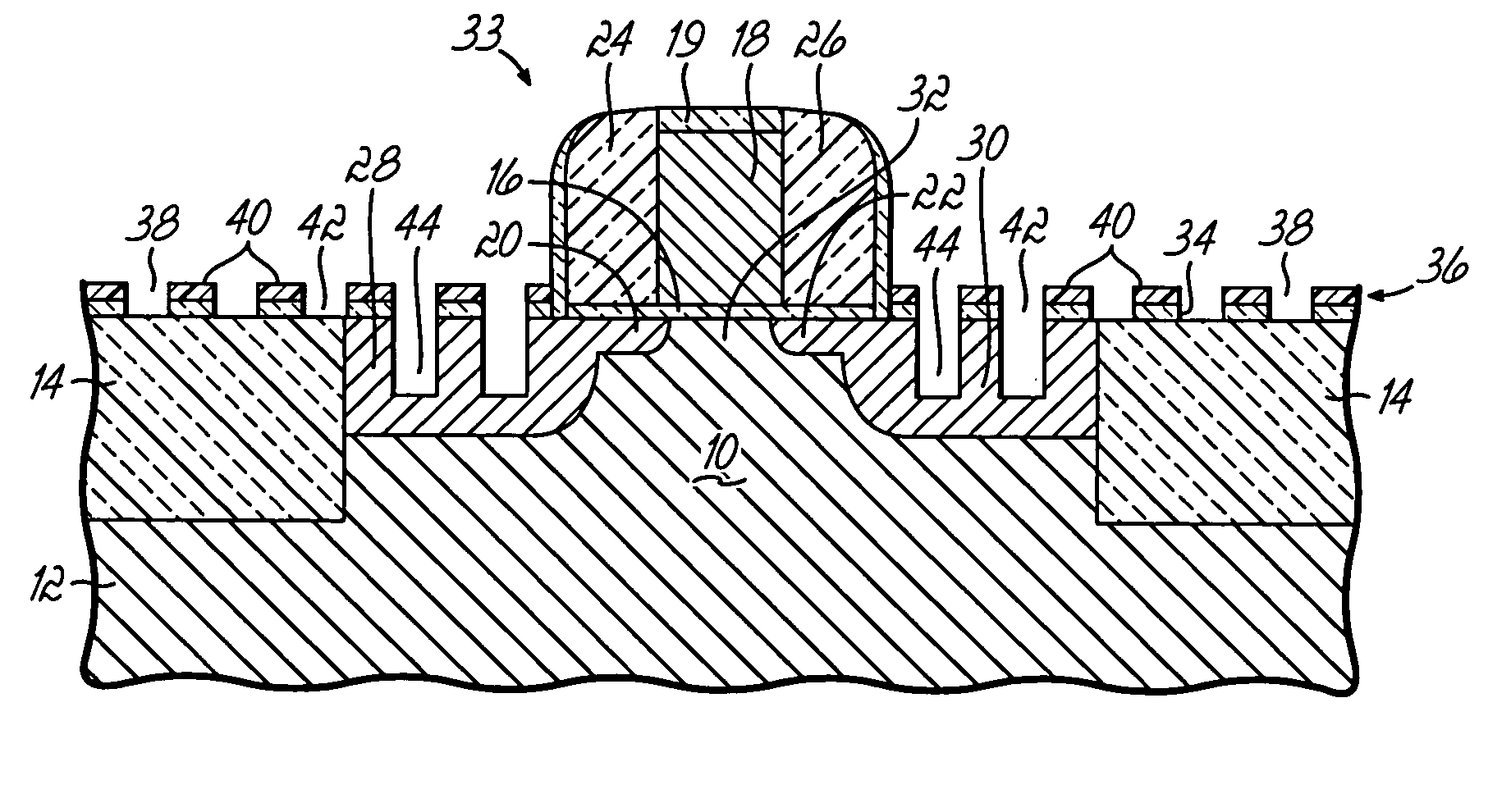
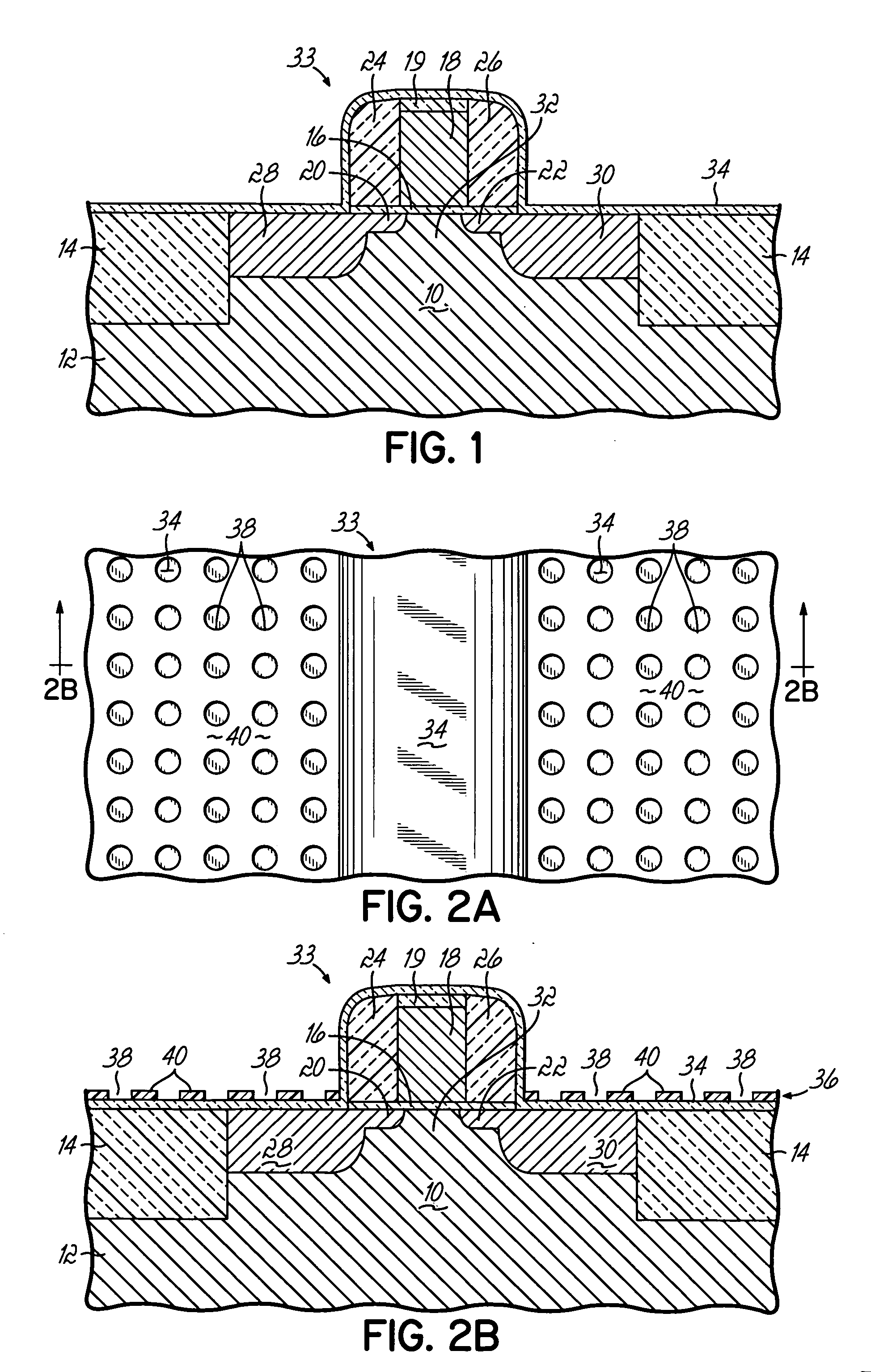
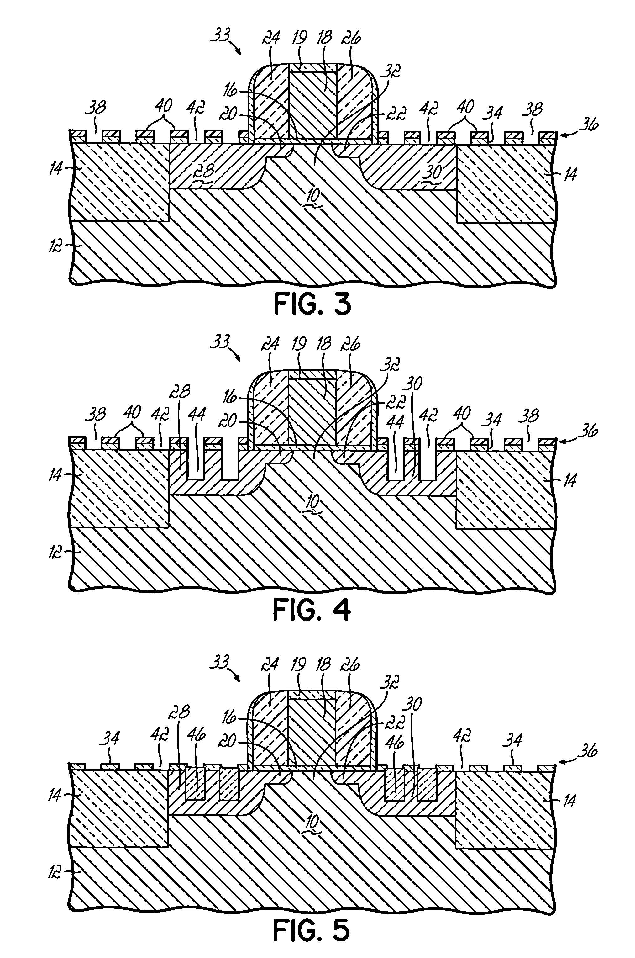
[0019] With reference to FIG. 1, a number of body regions, of which a single body region 10 is depicted, are defined in a substrate 12 of a suitable semiconductor material such as silicon. Substrate 12 may be, for example, a bulk substrate or the active layer of a silicon-on-insulator (SOI) substrate. Adjacent body regions 10 are isolated electrically by shallow trench isolation (STI) regions 14. The STI regions 14 are formed by conventional STI isolation techniques, such as defining trenches in substrate 12, filling the trenches with a dielectric material like silicon dioxide (SiO2) deposited by chemical vapor deposition, and planarizing to remove excess dielectric material by chemical-mechanical polishing (CMP) or any other suitable planarization technique such as an etch back process. The upper horizontal surfaces of the body regions 10 and the STI regions 14 are approximately level after planarization. It will be appreciated that other device isolation techniques, such as field ...


PUM


Abstract

Semiconductor fabrication methods and structures, devices and integrated circuits characterized by enhanced operating performance. The structures generally include first and second source / drain regions formed in a body of a semiconductor material and a channel region defined in the body between the first and second source / drain regions. Disposed in at least one of the first and second source / drain regions are a plurality of plugs each formed from a volume-expanded material that transfers compressive stress to the channel region. The compressively strained channel region may be useful, for example, for improving the operating performance of p-channel field effect transistors (PFET's).

Description

FIELD OF THE INVENTION [0001] The invention relates generally to semiconductor structures and devices and to a method for their fabrication and, more particularly, to fabrication methods and structures, devices and integrated circuits characterized by enhanced operating performance. BACKGROUND OF THE INVENTION [0002] Semiconductor devices, such as field effect transistors (FET's), are familiar building blocks of integrated circuits. Field effect transistors are formed from an electrically isolated body of semiconductor material, such as silicon, defined in a semiconductor substrate and include a channel region defined in the semiconductor body between a source region and a drain region. Carrier mobility in the channel region is an important consideration because of its direct influence on device performance. For example, transistor output current and switching performance may be improved by enhancing the carrier mobility in the channel region. One approach for enhancing the carrier ...

Claims


Application Information

Patent Timeline
Patent Type & Authority Applications(United States)
IPC IPC(8): H01L29/76
CPCH01L29/165H01L29/41725H01L29/665H01L29/6659H01L29/66636H01L29/78H01L2924/0002H01L29/7833H01L29/7848H01L23/485H01L2924/00H01L29/0847H01L29/0653
Inventor FURUKAWA, TOSHIHARUHAKEY, MARK CHARLESHOLMES, STEVEN JOHNHORAK, DAVID VACLAVKOBURGER, CHARLES WILLIAM III
Owner GLOBALFOUNDRIES INC
Why Eureka
Try Eureka