

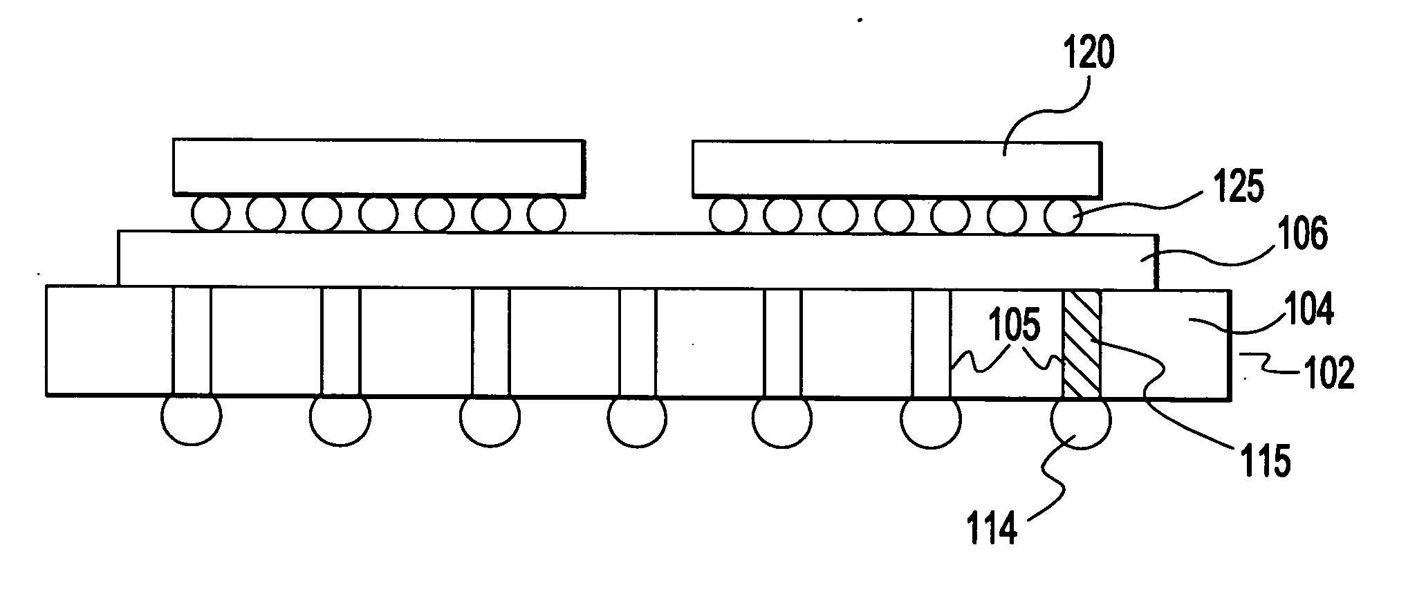
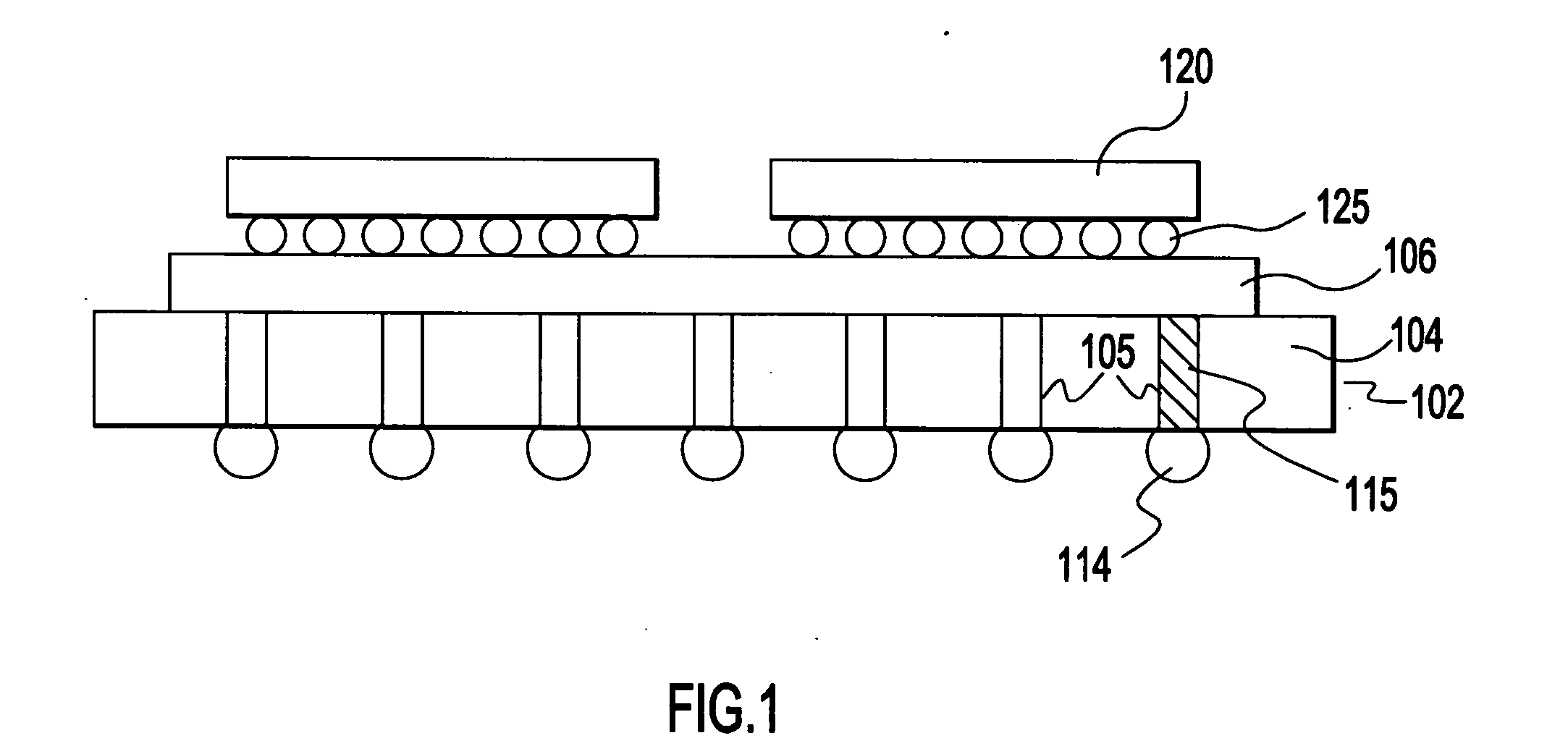
Silicon chip carrier with conductive through-vias and method for fabricating same
a silicon chip and through-via technology, applied in semiconductor devices, semiconductor/solid-state device details, electrical apparatuses, etc., can solve problems such as inability to control dimensional tolerances, material limitations, and inability to manufacture, and achieve the effects of reducing the number of through-vias
- Summary
- Abstract
- Description
- Claims
- Application Information
AI Technical Summary
Benefits of technology
Problems solved by technology
Method used
Image

Examples
second embodiment
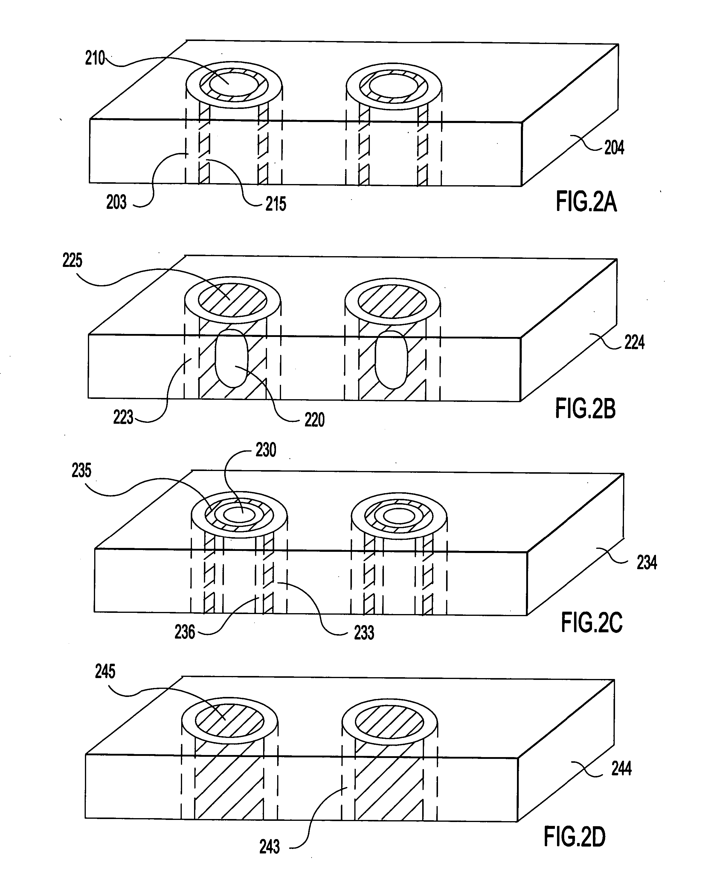
[0048]FIG. 5 is a flow chart of a representative process flow for fabricating a carrier with through-vias, as shown in FIG. 2B, in accordance with the present invention. At step 500, blind vias are etched into the substrate, as above, to a depth which is slightly greater than the desired depth of the through-vias in the finished product. At step 502, the sidewalls of the blind vias are insulated (as above), preferably by oxidizing silicon to form a thin layer of SiO2 or PECVD oxide or nitride or both. An annular fill is conducted at step 504 to provide metal (e.g., PVD TaN / Ta / Cu plus plated Cu to thickness ˜ 1 / 10 to ·⅕ of the via diameter) along the exposed insulated surfaces of the blind via. The top of the via is then capped with metal by either an overfilling, burnishing, or similar technique. The void in the center of the via will contain the ambient of the capping process, typically N2 or a vacuum. Overfilling is achieved by a PVD, CVD, evaporation, or sputtering process for me...
third embodiment
[0051]FIG. 7 is a flow chart of a representative process flow for fabricating a carrier with through-vias, as shown in FIG. 2C, in accordance with the present invention. At step 700, blind vias are etched into the substrate to a depth which is the desired depth of the through-vias in the finished product. The vias are etched in a pattern whereby each is an annular via of thickness ˜ 1 / 10 to ˜⅕ of the via diameter etched about a post of substrate material which will remain as the core of the via. At step 702, the sidewalls of the blind vias are insulated, preferably by oxidizing silicon to form a thin layer of SiO2 (see above) on both the outer sidewalls and the post sidewalls. The annular vias are then overfilled with the desired conductive material at step 704. Thereafter, the top of the structure is planarized at step 708 to remove excess metal at the top surface and to expose the substrate between the annular metal rings of the vias. IC circuits or components may be fabricated on...
PUM
| Property | Measurement | Unit |
|---|---|---|
| elastic modulus | aaaaa | aaaaa |
| temperatures | aaaaa | aaaaa |
| temperatures | aaaaa | aaaaa |
Abstract
Description
Claims
Application Information