
Temperature sensor insensitive to device offsets with independent adjustment of slope and reference temperature

a temperature sensor and offset technology, applied in the field of communication systems, can solve problems such as errors, and achieve the effects of reducing the accuracy of measurement irrecoverably, reducing the offset of amplifiers at the potential cost of complexity, and reducing the area of the di

Inactive Publication Date: 2006-02-09
AVAGO TECH WIRELESS IP SINGAPORE PTE
View PDF2 Cites 21 Cited by
  • Summary
  • Abstract
  • Description
  • Claims
  • Application Information

AI Technical Summary

Benefits of technology

[0014] While there are many ways of generating a PTAT signal in the prior art including using an analog amplifier to measure the two voltage terms of two diodes at different current densities and performing subtraction and amplification to generate the PTAT, such methods result in error being introduced due to device mismatch. Thus, the present invention includes circuitry and a method that eliminates error from device mismatch. The method and circuitry according to the various embodiments of the proposed invention include a design that facilitates sampling a single diode voltage drops based on differing current levels and feeding the measured voltage drops into a data converter and, finally, performing a temperature computation with digital logic to perform temperature based compensation.
[0015] The immunity of the invention to device mismatch impairments provides for a more robust and accurate temperature sensor. Furthermore the output is more readily utilized in a digital signal processing system as the output is already digitized.
[0018] Previous temperature sensors using analog components are subject to errors arising from device mismatch. For example, if a current density ratio of 16 is used to generate the two diodes voltages, the resulting difference voltage will be only 26 mV*ln(16) or about 72 mV. This is a difficult quantity to process with an analog amplifier where typical offsets may be on the order of 10-20 mV. The offset of the amplifier will then present an error to the system that will vary from part to part and degrade the accuracy of the measurement irrecoverably. For this reason, the offset of the amplifier is minimized at the potential cost of complexity, die area, and power.
[0019] A discrete-time switched-capacitor amplifier can overcome offset issues by sampling and canceling the offset in between sampling and amplifying the diode voltages. This method has proven to be suitable for highly accurate sensors but at the cost of considerable complexity.
[0021] In one application, a radio frequency (RF) variable gain amplifier (VGA) includes a power amplifier in a direct conversion radio transceiver that includes a gain determination module that reduces an input gain level to the power amplifier (PA) to reduce an output power level of the power amplifier according to temperature indications. In one embodiment of the invention, the gain determination module adjusts input gain levels to compensate for power reduction that occurs as a result of increased temperatures so as to maintain a constant output power level. In another embodiment of the invention, or alternative, in another mode of operation of the invention, the gain determination module reduces the input gain level to the power amplifier to prompt it to produce lower output power so as to cause it to reduce its operational temperature and, therefore, to maintain highest reliability.

Problems solved by technology

While there are many ways of generating a PTAT signal in the prior art including using an analog amplifier to measure the two voltage terms of two diodes at different current densities and performing subtraction and amplification to generate the PTAT, such methods result in error being introduced due to device mismatch.

Method used


Image

  • Temperature sensor insensitive to device offsets with independent adjustment of slope and reference temperature
  • Temperature sensor insensitive to device offsets with independent adjustment of slope and reference temperature
  • Temperature sensor insensitive to device offsets with independent adjustment of slope and reference temperature

Examples


Embodiment Construction

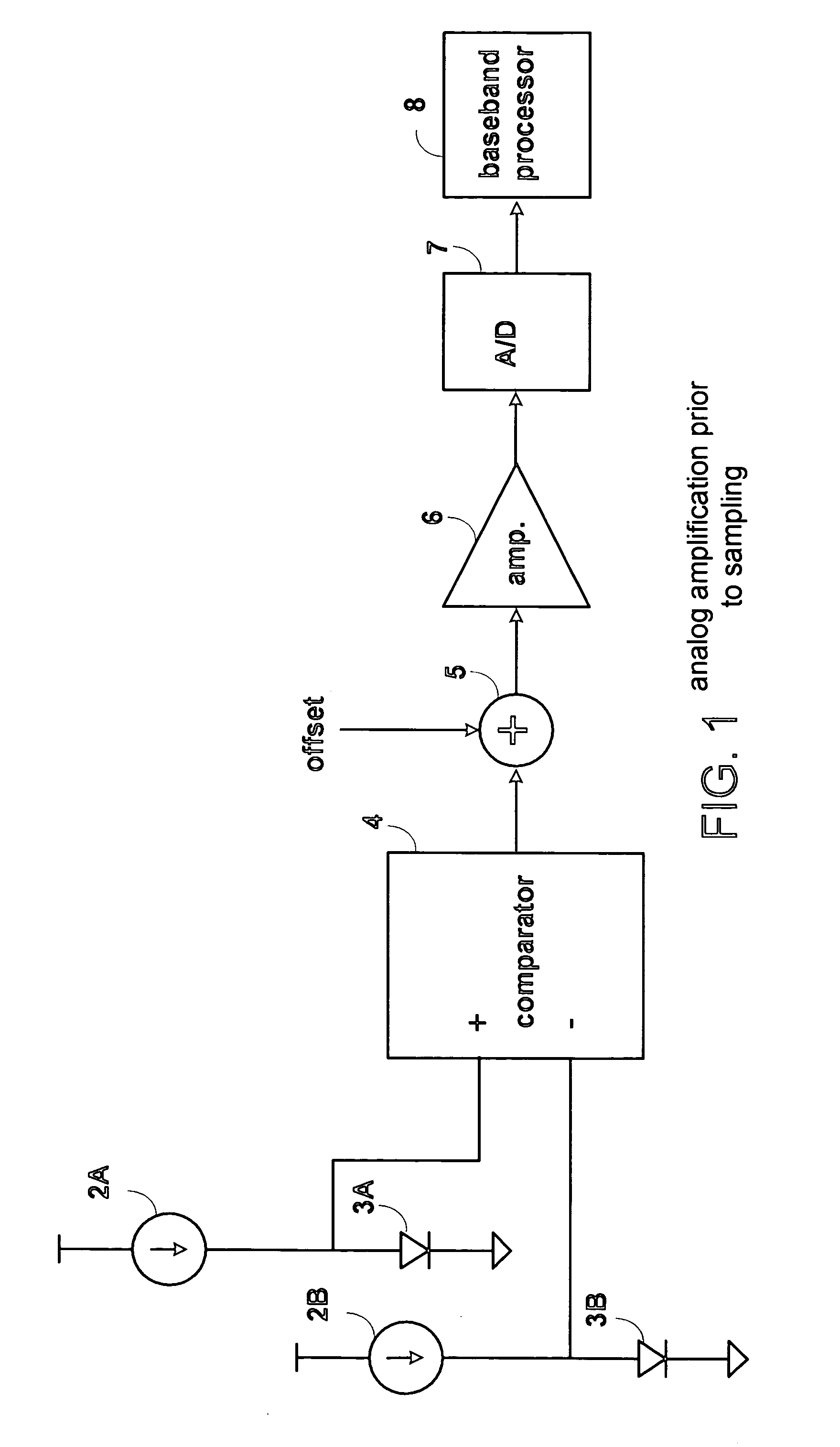
[0042]FIG. 1 is a functional schematic block diagram of a temperature sensor with amplification prior to sampling. As may be seen, a plurality of current sources 2A and 2B produce a current into diodes 3A and 3B, respectively. Voltage drops across the anode of diodes 3A and 3B are produced to plus and minus inputs of a comparator 4 which produces a difference of the voltage drops to an adder 5 which is further coupled to receive an offset signal. A sum of the offset signal and the difference of the voltage drops is then produced to an amplifier 6. An amplified signal produced by amplifier 6 is then produced to an analog-to-digital converter 7 which produces a digital value reflecting a temperature difference of diodes 3A and 3B. A processor 8 then produces temperature compensation to modify a specified device's operational range based upon the digital value reflecting the temperature difference (and therefore a temperature of the diode 3A or 3B that is being used as a temperature se...


PUM


Abstract

A radio transceiver includes circuitry that enables received RF signals to be down-converted to baseband frequencies and baseband signals to be up-converted to RF signals prior to transmission without requiring conversion to an intermediate frequency. The circuitry includes a temperature sensing module that produce accurate voltage level readings may be mapped into corresponding temperature values. A processor, among other actions, adjusts gain level settings based upon detected temperature values. One aspect of the present invention further includes repetitively inverting voltage signals across a pair of semiconductor devices beings used as temperature sensors to remove a common mode signal to produce an actual temperature-voltage curve. In one embodiment of the invention, the circuitry further includes a pair of amplifiers to facilitate setting a slope of the voltage-temperature curve.

Description

CROSS-REFERENCE TO RELATED APPLICATIONS [0001] This application claims priority to and incorporates by reference U.S. Utility Application entitled, “Local Oscillator Frequency Correction in a Direct Conversion RF Transceiver” having a Ser. No. 10 / 255,378 and a filing date of Sep. 26, 2002, and U.S. Utility Application entitled, “A Direct Conversion RF Transceiver For Wireless Communications”, having a Ser. No. 10 / 052,870 and a filing date of Jan. 18, 2002, and U.S. Utility Application entitled, “RF Variable Gain Amplifier With Fast Acting DC Offset Cancellation”, having a Ser. No. 10 / 274,655 and a filing date of Oct. 21, 2002.BACKGROUND [0002] 1. Technical Field [0003] This invention relates generally to communication systems and, more particularly, to Radio Frequency (RF) signal amplification within wireless devices operating in wireless communication systems. [0004] 2. Related Art [0005] Communication systems are known to support wireless and wire lined communications between wire...

Claims


Application Information

Patent Timeline
Patent Type & Authority Applications(United States)
IPC IPC(8): H01Q11/12H04M1/00
CPCH03F1/0205H03F1/30H03F2200/294H04B1/30H03F2200/447H04B1/036H03F2200/372
Inventor BEHZAD, ARYA REZAKAPPES, MICHAEL STEVEN
Owner AVAGO TECH WIRELESS IP SINGAPORE PTE
Learn More