High strain glass/glass-ceramic containing semiconductor-on-insulator structures

a technology of glass or glass-ceramic and semiconductor, which is applied in the field of semiconductor-on-insulator structures, can solve the problems of difficult replacement of silicon wafers with glass or glass-ceramic of the type, quartz itself is a relatively expensive material, and the cost of such structures has been etc., to achieve the effect of reducing the cost of silicon wafer replacement, reducing the cost of silicon wafers, and minimizing substrate compaction

Inactive Publication Date: 2006-02-23
CORNING INC
View PDF26 Cites 64 Cited by
  • Summary
  • Abstract
  • Description
  • Claims
  • Application Information

AI Technical Summary

Benefits of technology

[0018] The semiconductor-on-insulator structures and methods for making semiconductor-on-insulator structures of the present invention result in a number of advantages over prior art. The present invention satisfies the longstanding need in the art for lower cost substrates for use in high performance and electronic applications, when compared to fused silica or quartz based SIO structures. More particularly, the incorporation of the high strain point glass or glass-ceramic allows the SI

Problems solved by technology

To date, a major part of the cost of such structures has been the cost of the silicon wafer which supports the oxide layer, topped by the Si thin film, i.e., a major part of the cost has been the support substrate.
Although the use of quartz as a support substrate has been mentioned in various patents (see U.S. Pat. Nos. 6,140,209; 6,211,041; 6,309,950; 6,323,108; 6,335,231; and 6,391,740), quartz is itself a relatively expensive material
In particular, it is difficult to replace a silicon wafer with a glass or glass-ceramic of the type which can be manufactured in large quantities at low cost, i.e., it is difficult to make cost effective SOG structures.
Although these oxide glass or an oxide glass-ceramic based SOI structures were an improvement over the aforementioned prior art SOI structures, the glasses utilized in this oxide glass oxide glass or an o

Method used


Image

  • High strain glass/glass-ceramic containing semiconductor-on-insulator structures
  • High strain glass/glass-ceramic containing semiconductor-on-insulator structures
  • High strain glass/glass-ceramic containing semiconductor-on-insulator structures

Examples


example 1

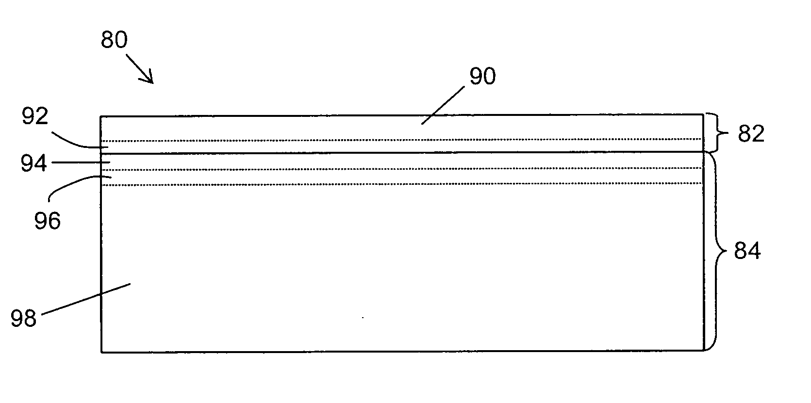
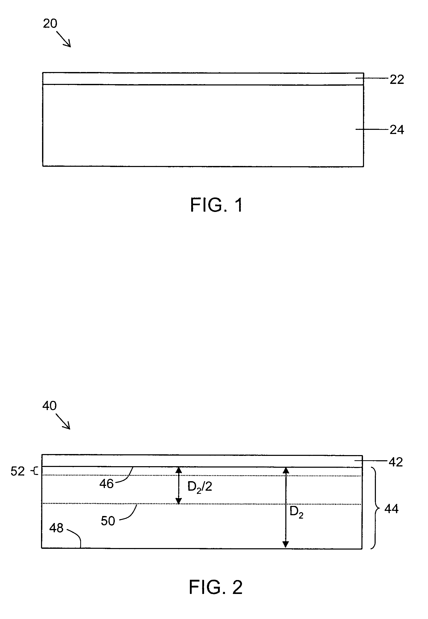
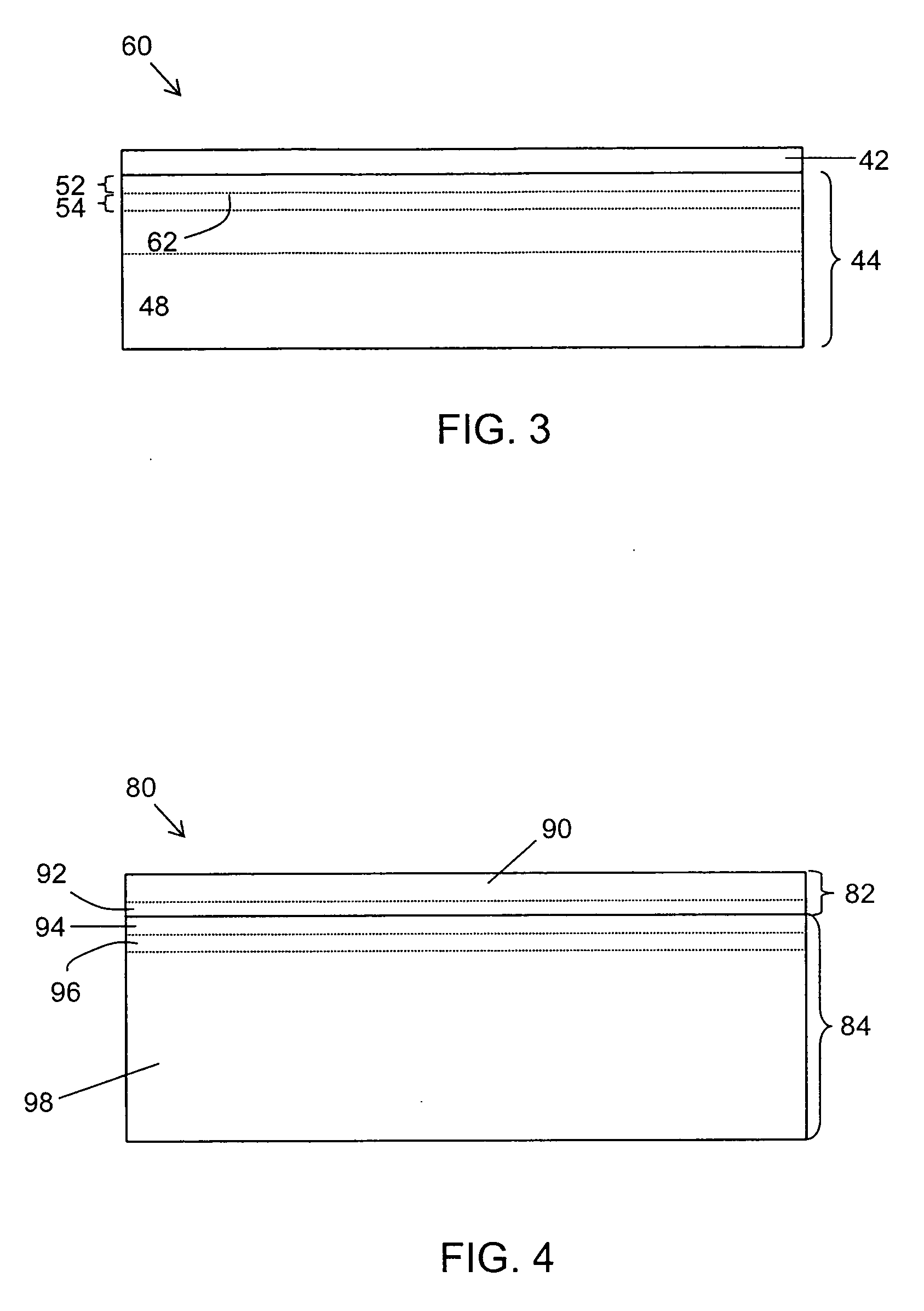
[0118] A 100 mm diameter, 1 mm thick wafer of glass 2N of Table 2, containing about 1 mole % of a Na2O dopant as calculated on an oxide basis, was fine ground and polished. A silicon wafer 525 μm in thickness was implanted with hydrogen at 100 keV and an ion dosage of 8×10¹⁶ ions / cm2 was cleaned with detergent and distilled water followed by a 10% nitric acid wash, and brought into contact with the glass wafer in a SUSS MICROTEC bonder. The glass wafer was heated at 450° C. and the silicon wafer at 400° C. in vacuum, and 10 psi pressure and 1750 V potential difference (glass at ground, silicon wafer at 1750 V) was applied for five minutes. While under the same potential difference and pressure, the glass wafer was heated at 575° C. and the silicon wafer at 525° C. for ten minutes, after which time the potential difference and pressure were removed, and the bonded wafers allowed to cool down. The cooled wafers separated into a silicon-on-glass wafer with a thin silicon layer, and a s...

example 2

[0119] A 100 mm diameter, 1 mm thick wafer of the glass-ceramic of 4A of Table 4, containing about 0.9 mole % Na2O dopant as calculated on an oxide basis, was fine ground and polished. A silicon wafer 525 μm in thickness was implanted with hydrogen at 100 keV and an ion dosage of 8×10¹⁶ ions / cm2 was cleaned with detergent and distilled water followed by a 10% nitric acid wash, and brought into contact with the glass wafer in a SUSS MICROTEC bonder. The glass wafer was heated at 450° C. and the silicon wafer at 400° C. in vacuum, and 10 psi pressure and 1750 V potential difference (glass at ground, silicon wafer at 1750 V) was applied for five minutes. While under the same potential difference and pressure, the glass wafer was heated at 575° C. and the silicon wafer at 525° C. for ten minutes, after which time the potential difference and pressure were removed, and the bonded wafers allowed to cool down. The cooled wafers separated into a silicon-on-glass wafer with a thin silicon la...


PUM

PropertyMeasurementUnit
Percent by massaaaaaaaaaa
Thicknessaaaaaaaaaa
Lengthaaaaaaaaaa

Abstract

The present invention relates to semiconductor-on-insulator structures having strained semiconductor layers. According to one embodiment of the invention, a semiconductor-on-insulator structure has a first layer including a semiconductor material, attached to a second layer including a glass or glass-ceramic, with the strain point of the glass or glass-ceramic equal to or greater than about 800° C.

Description

BACKGROUND OF THE INVENTION [0001] 1. Field of the Invention [0002] The present invention relates generally to semiconductor structures, and more particularly to semiconductor-on-insulator structures and methods for making semiconductor-on-insulator structures. [0003] To date, the semiconductor material most commonly used in semiconductor-on-insulator structures has been silicon. Such structures have been referred to in the literature as silicon-on-insulator structures and the abbreviation “SOI” has been applied to such structures. The present invention relates to semiconductor-on-insulator structures in general, including silicon-on-insulator structures. [0004] For ease of presentation, the following discussion will at times be in terms of silicon-on-insulator structures. The references to this particular type of semiconductor-on-insulator structure are made to facilitate the explanation of the invention and are not intended to, and should not be interpreted as, limiting the invent...

Claims


Application Information

Patent Timeline
IPC IPC(8): H01L27/12
CPCC03C3/06H01L29/78603C03C3/095C03C3/097C03C3/11C03C10/00C03C10/0009C03C10/0018C03C10/0027C03C10/0036C03C10/0045H01L21/76254H01L21/84H01L27/1203H01L27/1214H01L27/1266H01L29/7842C03C3/085H01L27/12
Inventor AITKEN, BRUCE GARDINERDEJNEKA, MATTHEW JOHNGADKAREE, KISHOR PURUSHOTTAMPINCKNEY, LINDA RUTH
Owner CORNING INC
Why Eureka
Try Eureka