
Carbon nanotube device, process for producing the same and carbon nanotube transcriptional body

Active Publication Date: 2006-02-23
FUJIFILM BUSINESS INNOVATION CORP
View PDF5 Cites 27 Cited by
  • Summary
  • Abstract
  • Description
  • Claims
  • Application Information

AI Technical Summary

Benefits of technology

[0025] When the cross-linking agent has a property in which the cross-linking agents may prompt a polymerization reaction with each other (self-polymerizability), the connecting group may contain a polymer in which two or more cross-linking agents are connected. An interval between carbon nanotubes can be controlled to a size of the residue of the cross-linking agent used, so that a desired network structure of carbon nanotubes can be obtained with high reproducibility. Furthermore, reducing the size of the residue of the cross-linking agent enables the interval between carbon nanotubes to be structured in such a manner that the carbon nanotubes are extremely close to each other both electrically and physically.
[0082] In addition, in the applied example of the present invention, the step of patterning the carbon nanotube structure layer into a pattern corresponding to a desired device is preferably performed in advance on the temporary substrate through a method such as etching described above in the case where fine patterning is required. However, the present invention can also adopt another method involving: cutting the carbon nanotube structure layer together with the temporary substrate into a pattern corresponding to a desired device; attaching the cut pattern to the base body; and removing the temporary substrate. In each of the carbon nanotube devices obtained through the above methods, carbon nanotubes mutually cross-link to construct a network structure, so that connection between carbon nanotubes is certainly formed. At the same time, even in the case where the carbon nanotube structure layer is transferred onto any one of base bodies of various shapes, carbon nanotubes hardly rupture owing to the toughness and flexibility of a carbon nanotube. Thus, interconnection between carbon nanotubes can be maintained at a favorable level even after the transfer.

Problems solved by technology

However, there are physical limitations on the realization of a wiring having a size of the order of 10−9 m with a metal wiring.
In addition, the metal wiring involves a problem called migration.
In the structure, the orientation varies from crystal grain to crystal grain, so that a large number of defects are present at a grain boundary.
As a result, problems such as an increase in wiring resistance and disconnection occur (this phenomenon is referred to as “migration”)
However, it is extremely difficult to actually wire carbon nanotubes.
However, the technique requires much time and labor.
Therefore, the technique is suitable for fundamental studies but is not practical.
With this technique, carbon nanotubes may be wired in one direction, but it is difficult to wire carbon nanotubes in plural directions.
Thus, this technique is not realistic.
However, in the method, a carbon nanotube grows only in the direction perpendicular to the substrate.
However, the probability of cross-link is extremely low, and wiring at an arbitrary position is still difficult.
However, in each of those methods, a carbon nanotube is merely dispersed in a solvent before application, or is mixed with a binder before application.
Therefore, the carbon nanotube is insufficient in terms of performance such as a mechanical strength or electric conductivity, and is hardly used directly as an electrode or an electric circuit.
In addition, when one tries to process such a carbon nanotube deposit, carbon nanotubes scatter during the processing, so that the deposit cannot be processed into a desired shape.
On the other hand, in the latter example in JP 2002-503204 A, in the case where cross-linking is performed using an alkoxide, alkoxides together form a complicated cross-linking structure, so that it is difficult to densely arrange carbon nanotubes.
As a result, there is a possibility that problems such as a problem in that excellent characteristics of a carbon nanotube itself are obtained only accidentally occur.
In addition, not only electrical applications of the structure but also general applications thereof are restricted.

Method used


Image

  • Carbon nanotube device, process for producing the same and carbon nanotube transcriptional body
  • Carbon nanotube device, process for producing the same and carbon nanotube transcriptional body
  • Carbon nanotube device, process for producing the same and carbon nanotube transcriptional body

Examples


example 2

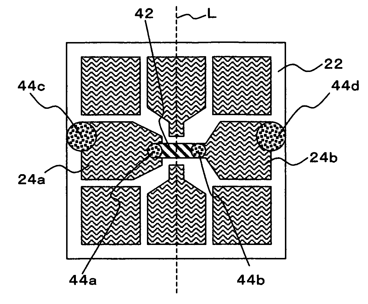
[0307] As shown in FIG. 10, an LED (manufactured by Stanley Electric Co., Ltd., DB1111C) 32 was mounted onto the carbon nanotube structure layers 14 (opposing end portions of 14a and 14b in FIG. 9) functioning as electrodes in the carbon nanotube device obtained in Example 1 with silver pastes 34a and 34b.

[0308] In addition, a lead wire (not shown) to be connected to a power supply device (not shown) was connected to the other end portions of the carbon nanotube structure layers 14a and 14b with silver pastes 34c and 34d, and the resultant was provided as an electrode terminal, thereby obtaining a carbon nanotube device of Example 2. Here, FIG. 2 is an enlarged plan view of the surface of the carbon nanotube device of Example 2.

[0309] A voltage was applied to the electrode terminal with the power supply device, with the result that the LED 32 lighted up at 3.3 V. The result confirmed that circuit formation was performed.

example 3

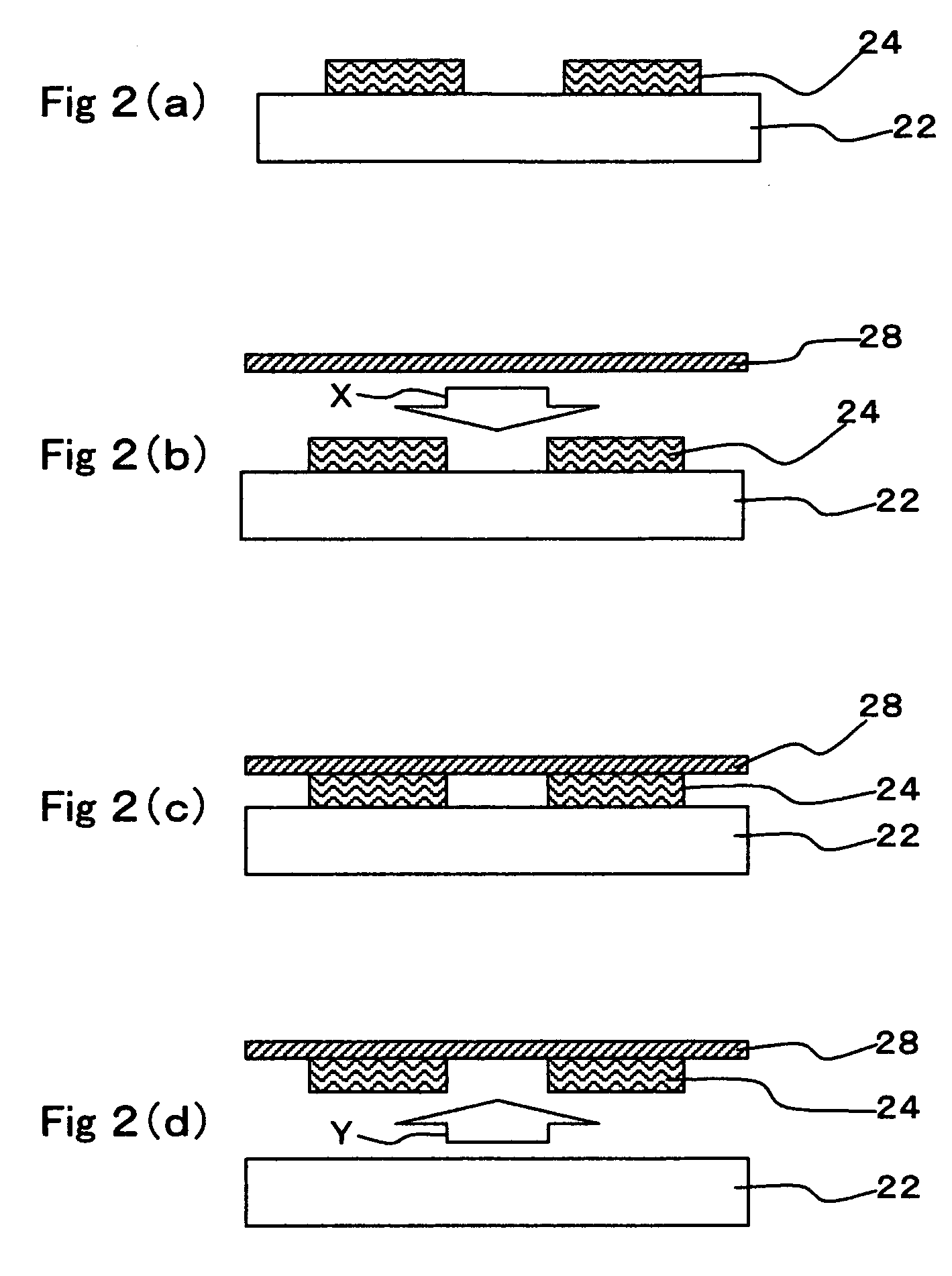
[0315] A carbon nanotube device was manufactured according to the flow of the method of manufacturing a carbon nanotube device shown in FIG. 2 (applied example). In some cases, reference numerals in FIG. 2 are used in the description of this example.

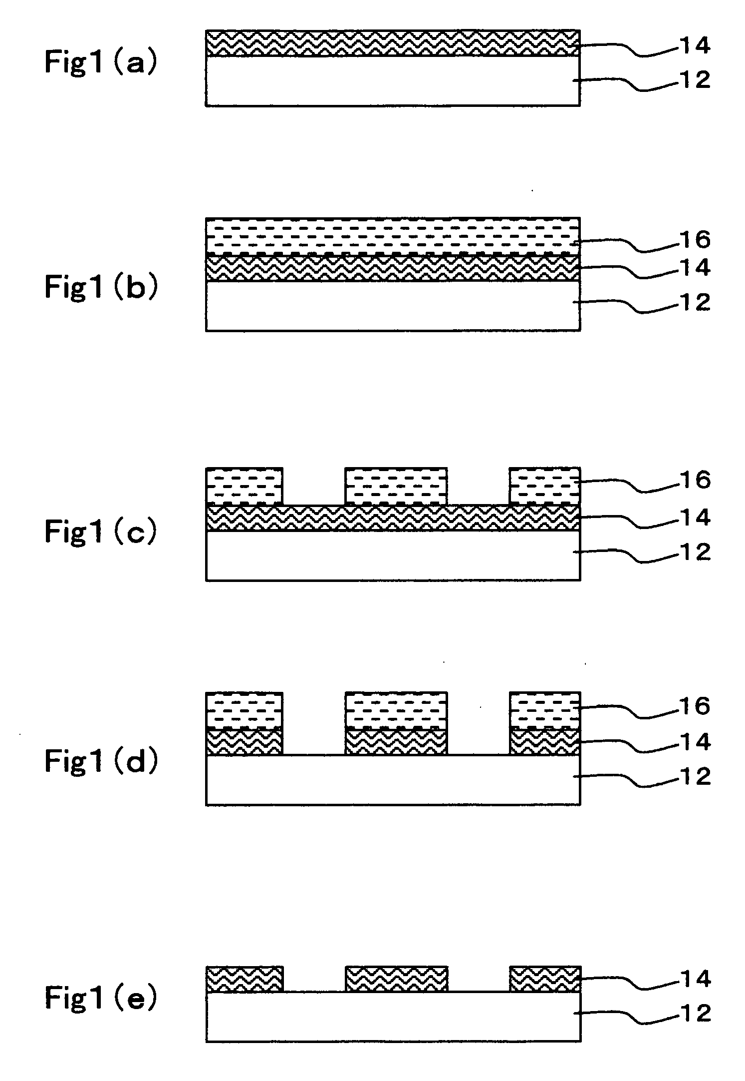
(A) Applying Step, (B) Cross-linking Step, and (C) Patterning Step

[0316] The operations of (A) Applying Step, (B) Cross-linking Step, and (C) Patterning Step were performed in the same manner as in Example 1 to prepare a product in a state shown in FIG. 2(a). In this example, the silicon wafer used in Example 1 corresponds to the temporary substrate 22, and a product formed in a predetermined pattern (shape of the carbon nanotube structure layer 14 of FIG. 9) on the surface of the temporary substrate 22 corresponds to the carbon nanotube structure layer 24.

(D) Transferring Step

[0317] In the silicon wafer on which the carbon nanotube structure layer 24 had been formed, an adhesive surface of an imide tape (available from Permacel, 1...


PUM


Abstract

To provide a carbon nanotube device capable of efficiently exerting various electrical or physical characteristics of a carbon nanotube, the present invention provides: a carbon nanotube device, in which a carbon nanotube structure layer having a network structure in which plural carbon nanotubes mutually cross-link, is formed in an arbitrary pattern on a surface of a base body; and a method of manufacturing the carbon nanotube device with which the carbon nanotube can be suitably manufactured.

Description

TECHNICAL FIELD [0001] The present invention relates to a carbon nanotube device useful for various electrical components and electrical elements or useful for various structures that utilize the toughness, thermal conductivity, and other characteristics of a carbon nanotube, a method of manufacturing the same, and to a carbon nanotube transfer body facilitating the manufacture of the carbon nanotube device. In particular, the present invention relates to a carbon nanotube device using carbon nanotubes for various electrical wirings or electrical components, the carbon nanotube device being extremely fine and excellent in electrical characteristics, a method of manufacturing the same, and to a carbon nanotube transfer body. BACKGROUND ART [0002] Carbon nanotubes (CNTs), with their unique shapes and characteristics, are being considered for various applications. A carbon nanotube has a tubular shape of one-dimensional nature which is obtained by rolling one or more graphene sheets co...

Claims


Application Information

Patent Timeline
IPC IPC(8): H01L21/4763H01L23/48B82B3/00B82B1/00C01B31/02H01L21/28H01L21/3205H01L23/52H01L29/06H01L51/00H01L51/05H01L51/30H01L51/40H01L51/52H05K1/09H05K3/06
CPCB82Y10/00B82Y30/00Y10S977/749B82Y40/00C01B31/0253C01B31/0273H01L51/0018H01L51/0023H01L51/0049H01L51/0508H01L51/0595H01L51/102H01L51/5203H01L2924/0002Y10S977/742Y10S977/726Y10S977/721H01L2924/00C01B32/168C01B32/174H10K71/233H10K71/621H10K85/225H10K10/46H10K10/82H10K10/701H10K50/805
Inventor HIRAKATA, MASAKIISOZAKI, TAKASHIKISHI, KENTAROSHIGEMATSU, TAISHIMANABE, CHIKARAANAZAWA, KAZUMORIWATANABE, HIROYUKISHIMIZU, MASAAKI
Owner FUJIFILM BUSINESS INNOVATION CORP
Learn More