Delay locked loop circuitry and method for optimizing delay timing in mixed signal systems

Inactive Publication Date: 2006-02-23
TEXAS INSTR INC
View PDF6 Cites 32 Cited by
  • Summary
  • Abstract
  • Description
  • Claims
  • Application Information

AI Technical Summary

Benefits of technology

[0015] It is an object of the invention an improved method and circuit for minimizing degr

Problems solved by technology

In such high-performance monolithic mixed signal systems, transitions of digital signals associated with digital circuitry often create a noise or disturbance (sometimes referred to as a “glitch”) that is superimposed on ground conductors and/or supply voltage conductors and/or signal conductors and/or the integrated circuit chip substrate.
Such noise or interference may degrade analog circuit performance, depending on the magnitude and timing of the glitch.
If a falling edge of a pulse of an analog clock signal that controls switch 80 occurs during the noise glitch 6, it could cause interference such as a ground bounce voltage to be superimposed the value of Vin that has just been sampled onto capacitor C as described above, and could cause inaccurate analog circuit operation.
This may result in unacceptable inaccuracy of the voltage produced by the output of integrating amplifier 83.
For example, even a error as low as a few microvolts can cause unacceptable error in a 24-bit ADC and substantially decrease the SNR (signal to noise ratio) of a system including the delta sigma ADC.
However, this approach is not viable in systems wherein the master clock signal is used directly for clocking either the digital circuitry or the analog circuitry.
A phase locked loop could usually be used to

Method used


Image

  • Delay locked loop circuitry and method for optimizing delay timing in mixed signal systems
  • Delay locked loop circuitry and method for optimizing delay timing in mixed signal systems
  • Delay locked loop circuitry and method for optimizing delay timing in mixed signal systems

Examples


Embodiment Construction

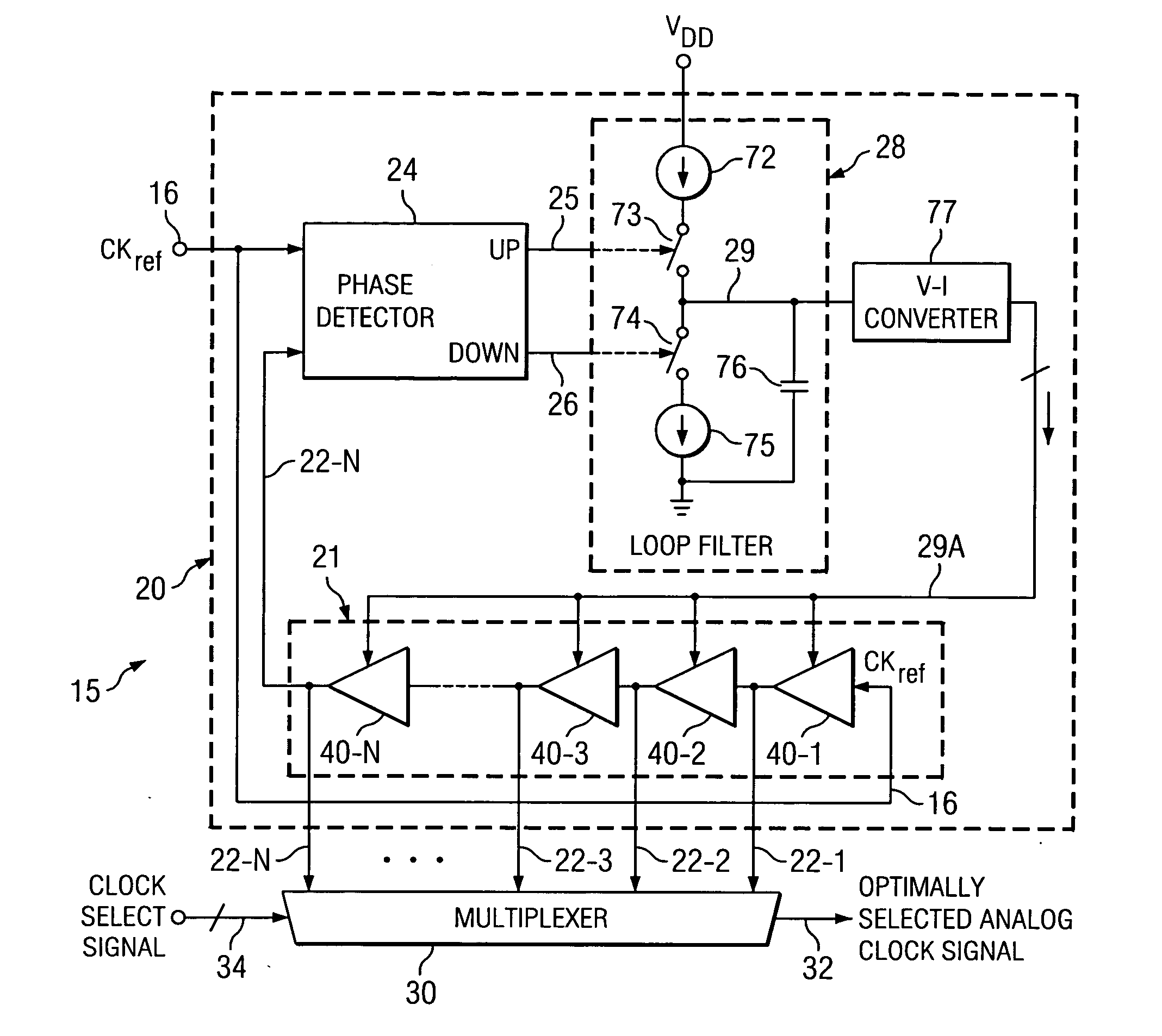
[0034] The described embodiment of the invention provides a practical way of selecting an optimum amount of the delay between an analog clock signal and a digital clock signal so as to reduce or minimize degradation of analog signals in a mixed signal systems due to noise caused by digital signals therein, wherein the delay is insensitive to temperature variations and process variations.

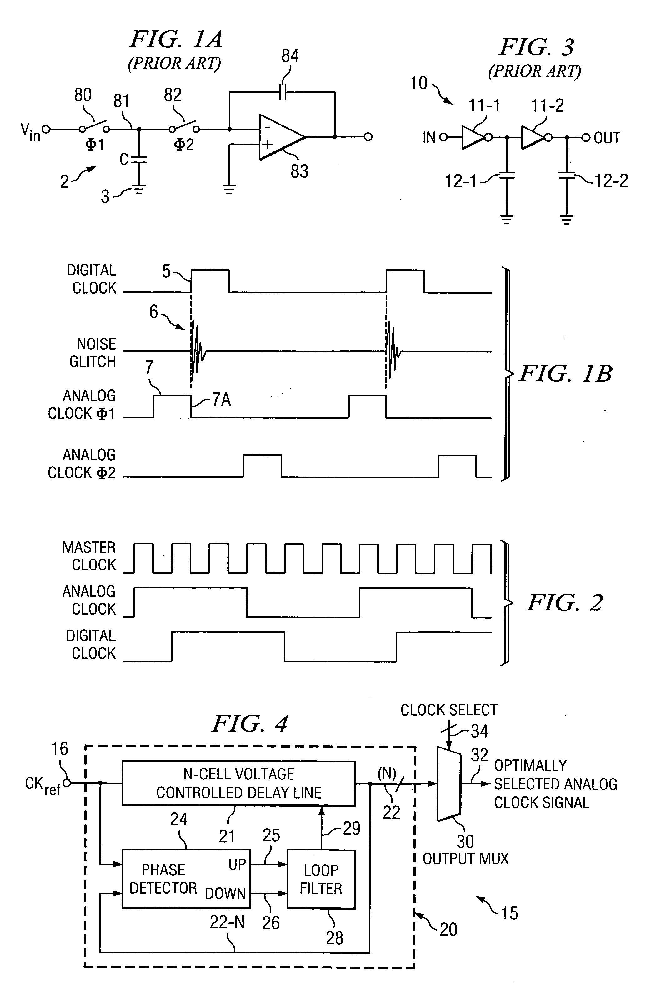
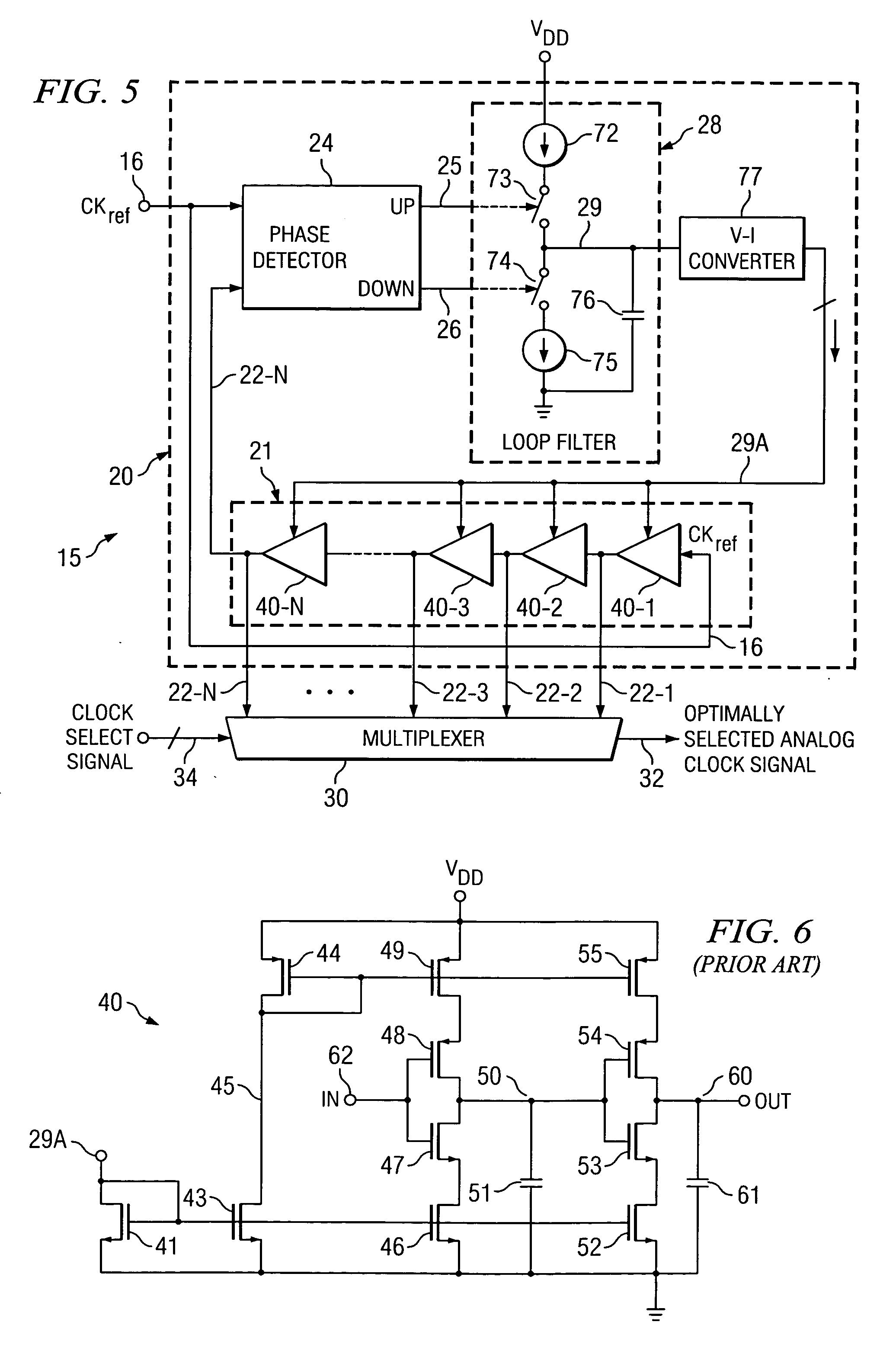
[0035] Referring to FIG. 4, an analog clock generation circuit 15 of the present invention includes a conventional delay locked loop (DLL) circuit 20 and an output multiplexer circuit 30. DLL circuit 20 includes a voltage controlled delay line 21 having N delay cells, a phase detector 24, and a loop filter 28. An input clock signal CKref is applied by conductor 16 to an input of the first delay cell 40-1 of controlled delay line 21 and also to a first input of phase detector 24. The outputs of the various N delay cells of controlled delay line 21 are connected to various inputs, respectively, of an ...


PUM


Abstract

A mixed signal system includes a digital circuit (17) clocked by a digital clock signal, an analog circuit (18) clocked by an analog clock signal, and clock generation circuitry (15) including a delay locked loop (20) including a N-cell delay line (21) having an input for receiving a reference clock signal and a plurality of delay outputs (22), and a multiplexer (30) having a plurality of inputs coupled to the plurality of delay outputs (22), respectively. A selection signal (34) causes the multiplexer (30) to couple a selected one of the delay outputs (22) to an output (32) of the multiplexer (30) so as to cause the analog clock signal and the digital clock signal to be sufficiently skewed from each other to minimize an inaccuracy in the analog circuit (18) caused by a noise glitch associated with the digital clock signal.

Description

BACKGROUND OF THE INVENTION [0001] The present invention relates generally to high-performance monolithic (i.e., integrated circuit) mixed signal systems including digital and also including analog circuitry, such as a low noise delta sigma analog-to-digital converter (ADC) and / or a digital-to-analog-converter (DAC). The invention relates more particularly to a method and circuit for minimizing the degradation of analog signals due to noise caused by digital signals in a monolithic mixed signal system. [0002] In such high-performance monolithic mixed signal systems, transitions of digital signals associated with digital circuitry often create a noise or disturbance (sometimes referred to as a “glitch”) that is superimposed on ground conductors and / or supply voltage conductors and / or signal conductors and / or the integrated circuit chip substrate. Such noise or interference may degrade analog circuit performance, depending on the magnitude and timing of the glitch. The timing of certa...

Claims


Application Information

Patent Timeline
IPC IPC(8): H03L7/06
CPCH03M1/0827H03L7/0812H03L7/0816
Inventor WANG, BINAN
Owner TEXAS INSTR INC
Why Eureka
Try Eureka