Gasless high voltage high contact force wafer contact-cooling electrostatic chuck

Inactive Publication Date: 2006-03-02
APPLIED MATERIALS INC
View PDF99 Cites 41 Cited by
  • Summary
  • Abstract
  • Description
  • Claims
  • Application Information

AI Technical Summary

Benefits of technology

[0008] The foregoing eliminates the need for any coolant gas in the electrostatic chuck, so that far more RF bias voltage may be applied through the chuck without arcing,

Problems solved by technology

For example, high temperatures can adversely affect the sharp semiconductor junction profiles required for small feature sizes.
In plasma processing of wafers, the wafer temperature can exceed many hundreds of degrees C., particularly where large RF bias power levels are employed at low chamber pressure, where heat transfer by gas convection and conduction is poor (and radiation heat transfer is also poor).
Unfortunately, such high gas pressure reduces the threshold RF power level (or RF voltage level) at which arcing, gas breakdown, or dielectric breakdown occurs within the helium gas passages in the chuck, in the interface between electrostatic chuck and wafer, or in the wafer support pedestal.
Such problems have become more critical as greater demands are placed on processes such as plasma immersion ion implantation processes.
Similar problems can occur in other applications, such as plasma or reactive ion etching etching, plasma chemical vapor deposition, physical vapor deposition, etc.
Another problem is that the top surface of the electrostatic chuck must have many open channels (channels machined into the chuck top surface) through which the helium cooling gas is pumped to provide thermal conductance between the wafer and the chuck.
Such channels have many sharp edges, which create contamination of particles on the wafer backside or contamination of the process.
Contamination is caused by scratching the wafer backside over the sharp edges of

Method used


Image

  • Gasless high voltage high contact force wafer contact-cooling electrostatic chuck
  • Gasless high voltage high contact force wafer contact-cooling electrostatic chuck
  • Gasless high voltage high contact force wafer contact-cooling electrostatic chuck

Examples


Embodiment Construction

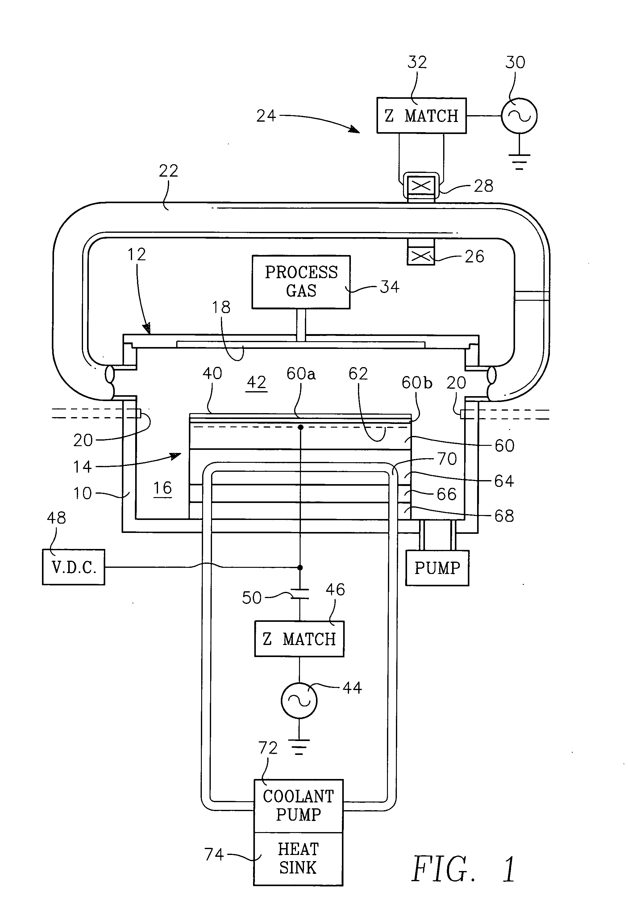
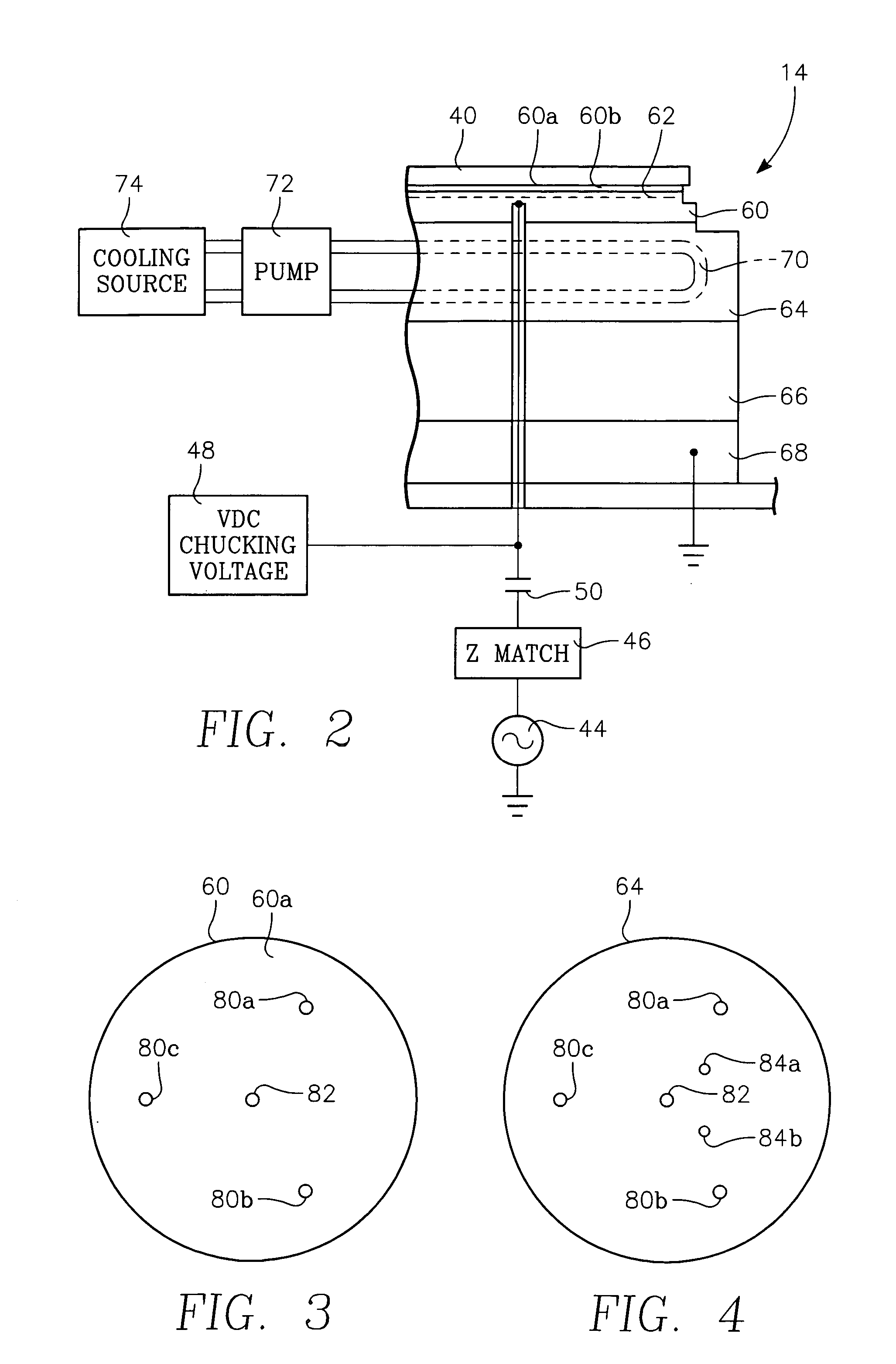
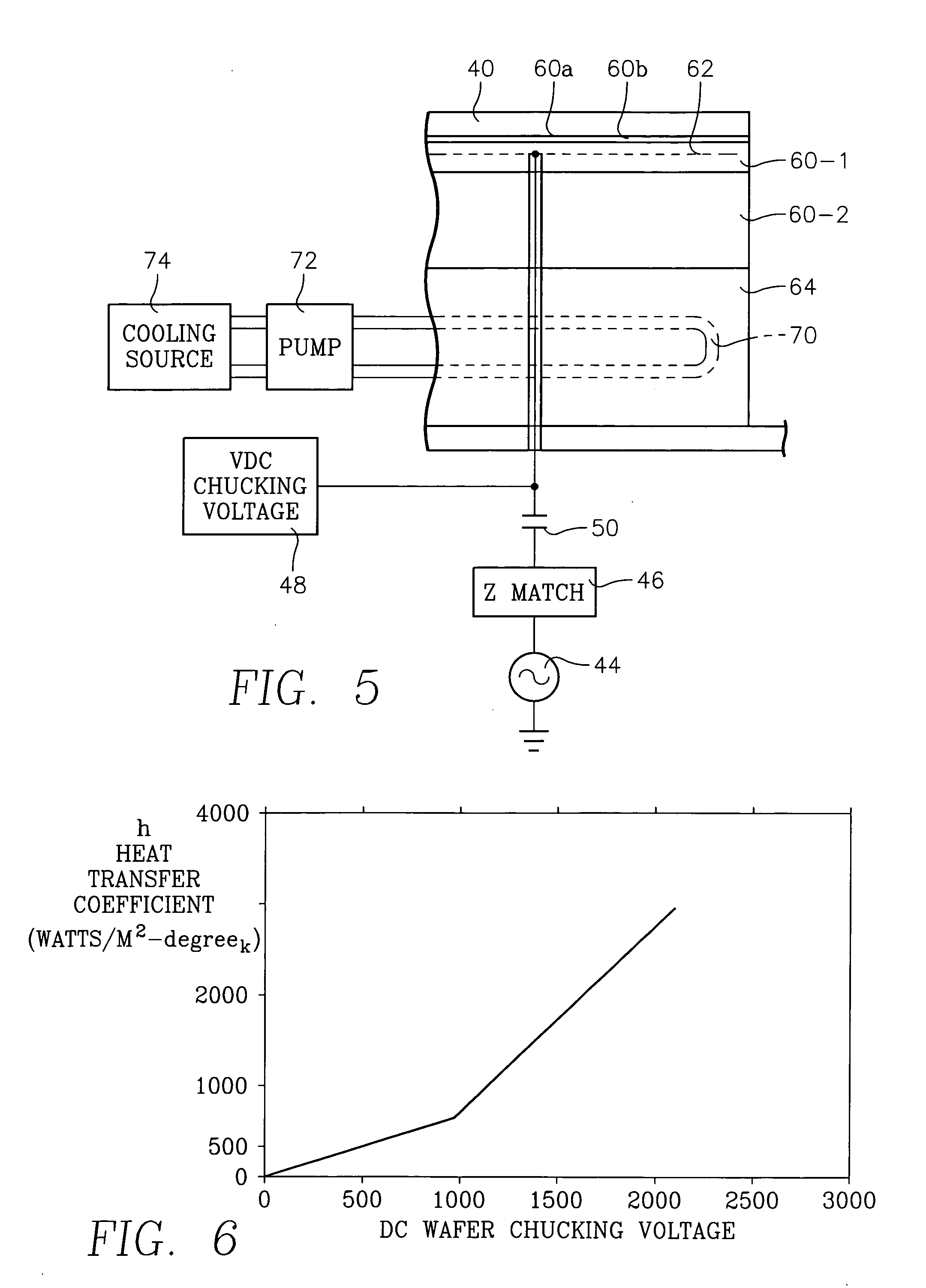
[0032]FIGS. 1 through 4 depict a plasma reactor with the wafer contact-cooling electrostatic chuck in accordance with certain embodiments of the invention. FIG. 1 is a cut-away side view of a plasma reactor for processing a semiconductor reactor that includes the wafer contact-cooling electrostatic chuck. FIG. 2 is a cross-sectional side view of the wafer contact-cooling electrostatic chuck. FIGS. 3 and 4 are top cross-sectional views of different layers of the wafer contact-cooling electrostatic chuck. In FIG. 1, the plasma reactor has a cylindrical side wall 10, a ceiling 12 and a wafer contact-cooling electrostatic chuck 14. A pumping annulus 16 is defined between the chuck 14 and the sidewall 10. While the wafer contact-cooling electrostatic chuck 14 may be used in any type of plasma reactor or other reactor (such as thermal process reactor), the reactor in the example of FIG. 1 is of the type in which process gases can be introduced through a gas distribution plate 18 (or “show...


PUM

PropertyMeasurementUnit
Fractionaaaaaaaaaa
Fractionaaaaaaaaaa
Fractionaaaaaaaaaa

Abstract

A method of electrostatically chucking a wafer while removing heat from the wafer in a plasma reactor includes providing a polished generally continuous surface on a puck, placing the wafer on the polished surface of the puck and cooling the puck. A chucking voltage is applied to an electrode within the puck to electrostatically pull the wafer onto the surface of the puck with sufficient force to attain a selected heat transfer coefficient between contacting surfaces of the puck and wafer.

Description

BACKGROUND OF THE INVENTION [0001] Semiconductor wafer processing requires more strict control of wafer temperature to reduce wafer temperature excursion during processing, as device geometries shrink to ever smaller dimensions. For example, high temperatures can adversely affect the sharp semiconductor junction profiles required for small feature sizes. Limiting workpiece (or semiconductor wafer) temperature during processing is also necessary whenever processing is carried out using photoresist masking of device features, in order to avoid heat-induced degradation of the photoresist. [0002] In plasma processing of wafers, the wafer temperature can exceed many hundreds of degrees C., particularly where large RF bias power levels are employed at low chamber pressure, where heat transfer by gas convection and conduction is poor (and radiation heat transfer is also poor). For example, in plasma immersion ion implantation reactors, RF bias power applied to the wafer may be many kWatts,...

Claims


Application Information

Patent Timeline
IPC IPC(8): B44C1/22
CPCH01L21/6831H01L21/67109
Inventor BUCHBERGER, DOUGLAS A. JR.HOFFMAN, DANIEL J.RAMASWAMY, KARTIKNGUYEN, ANDREWHANAWA, HIORJICOLLINS, KENNETH S.AL-BAYATI, AMIR
Owner APPLIED MATERIALS INC
Why Eureka
Try Eureka