Ion implanter having enhanced low energy ion beam transport

a low energy, ion beam technology, applied in the direction of irradiation devices, electric discharge tubes, electrical apparatus, etc., can solve the problems of reducing throughput, affecting throughput, and not being able to efficiently achieve the energies required,

Inactive Publication Date: 2006-03-02
VARIAN SEMICON EQUIP ASSOC INC
View PDF8 Cites 24 Cited by
  • Summary
  • Abstract
  • Description
  • Claims
  • Application Information

AI Technical Summary

Benefits of technology

[0021] According to a further aspect of the invention, a method for implanting ions in a target is provided. The method comprises generating an ion beam, separating unwanted components from the ion beam in an analyzer, transporting the ion beam through the analyzer at a first transport energy, decelerating the ion beam from the first transport energy to a second transport energy in a deceleration stage comprising two or more electrodes, wherein at least one of the electrodes comprises a grid electrode disposed in the beam path, and delivering the decelerated ion beam to a target site.

Problems solved by technology

However, ion implanters are typically designed for efficient operation at relatively high implant energies, for example in the range of 20 keV to 400 keV, and may not function efficiently at the energies required for shallow junction implantation.
As a result, extremely long implant times are required to achieve a specified dose, and throughput is adversely affected.
Such reduction in throughput increases fabrication cost and is unacceptable to semiconductor device manufacturers.
However, a small ion current is delivered to the wafer because the ion source operates inefficiently at low extraction voltages.
Ion beam transport is efficient at high energies and is less efficient at low energies due to effects of space charge neutralization loss and beam blowup.
These effects are particularly severe in regions of electrical fields, such as deceleration gaps needed to decelerate the beam from initial energies of beam generation and transport to the desired final lower energy.
A deceleration following a single magnet is accompanied by some level of beam contamination which results from beam which neutralizes either in residual gas or by small angle scattering from surfaces before the beam is decelerated to its final energy.
The result is impaired electrical performance of the devices being manufactured using the implanter.
The main obstacle to good performance is the efficiency of transport of the ion beam through the second magnet and to the wafer following its first deceleration.
Typically, an ion beam which is optimized for such a system may have severe aberrations due to transport in the first magnet, and the aberrant beams are difficult to match into the entrance aperture of the second magnet when the energy is low and the deceleration stage between the magnets is used.
The mismatch is exacerbated by small angle errors in centration (in the plane perpendicular to the analyzing magnet median plane) which result from magnetic fields in the ion source.
Correction of these errors using extraction manipulators to offset the extraction fields of the ion source only approximately corrects the angle.
This defect is minor at high energies when the beam is small in the direction of the error.
However, at low energies and also after deceleration and transport over a long distance, the angle error can prevent complete transmission through the second magnet.
In addition, beam blowup from space charge expansion in the deceleration region can cause overfill of the pole gap of the second magnet.
Beam efficiency suffers as a result.

Method used


Image

  • Ion implanter having enhanced low energy ion beam transport
  • Ion implanter having enhanced low energy ion beam transport
  • Ion implanter having enhanced low energy ion beam transport

Examples


first embodiment

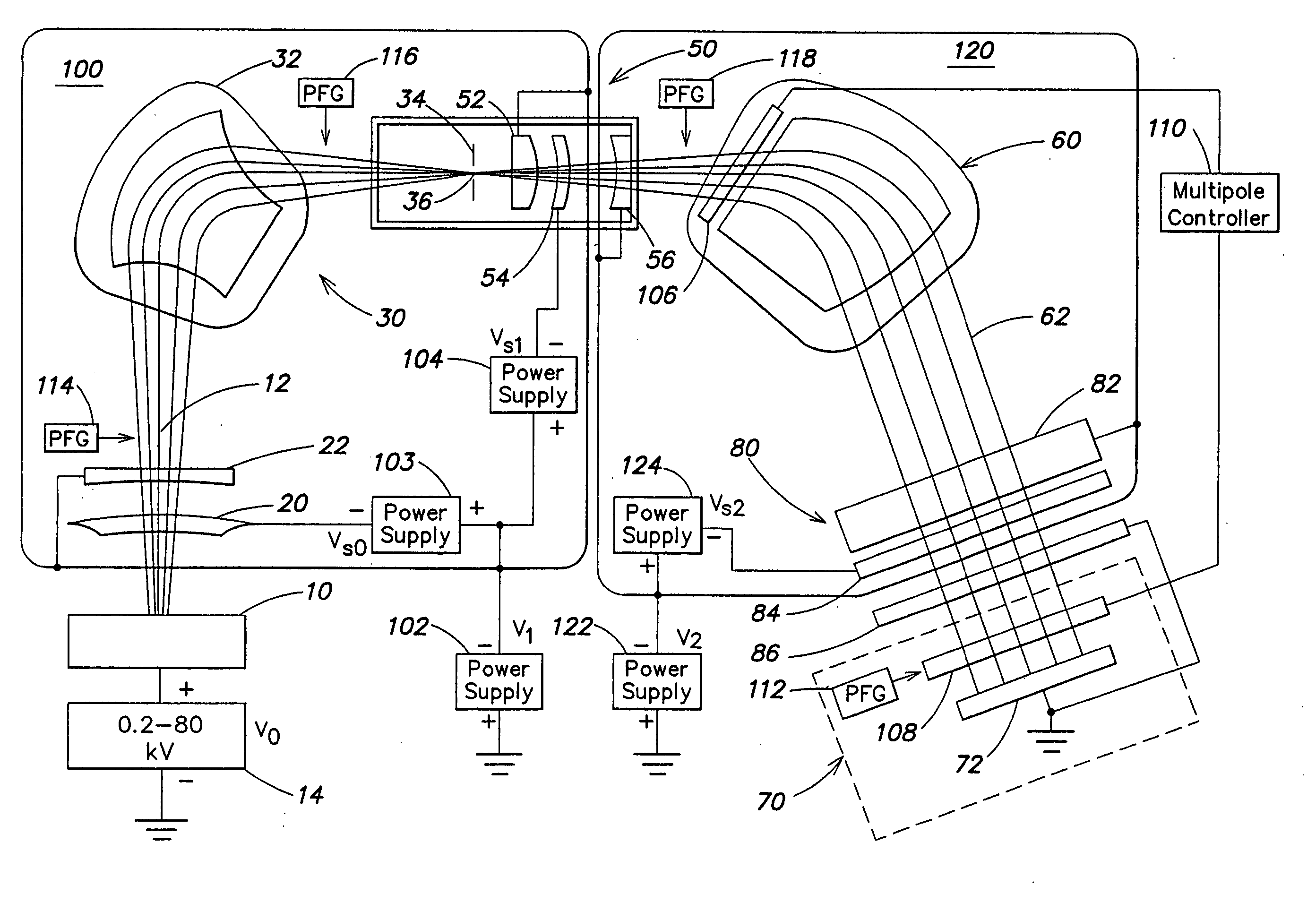
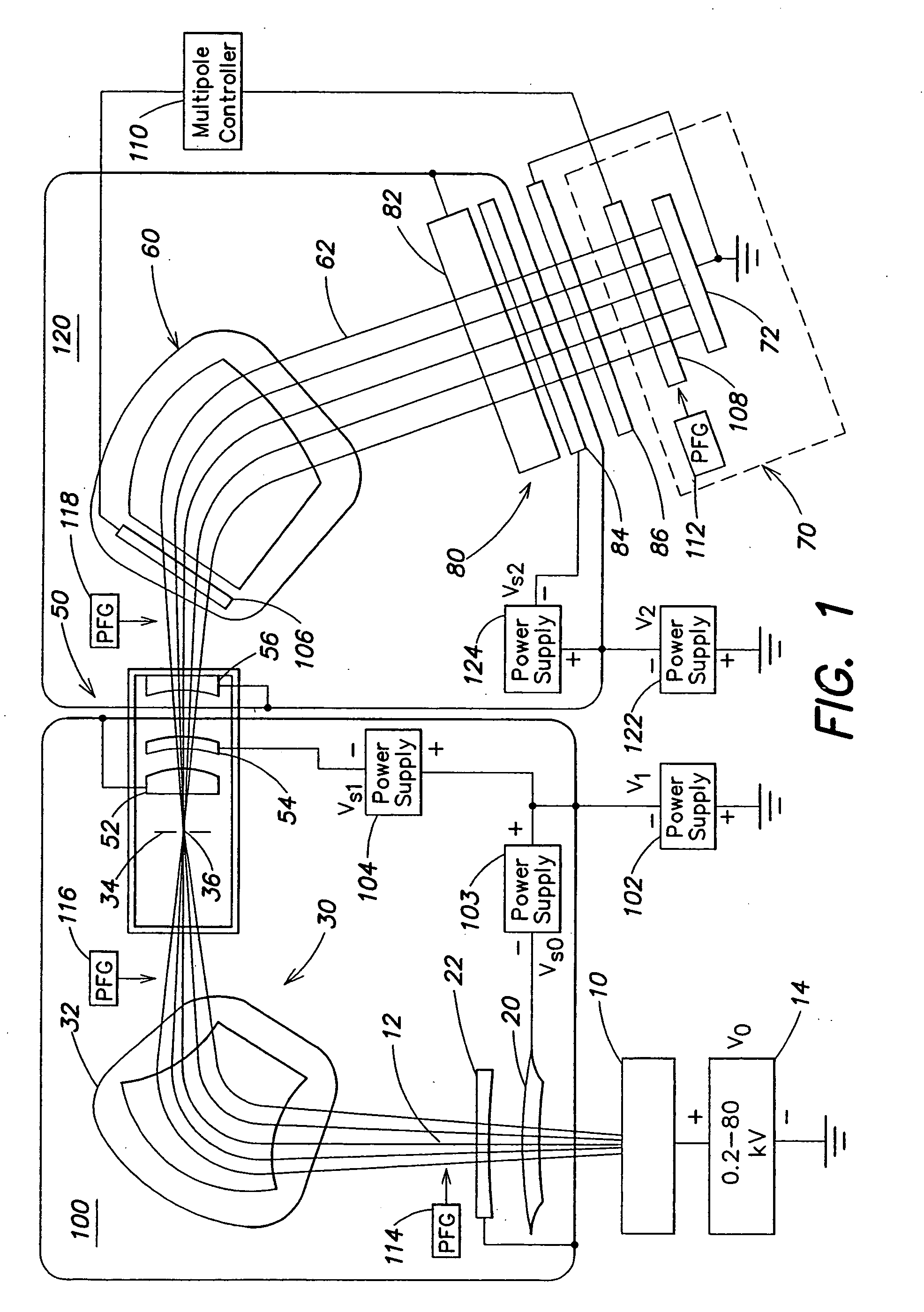
[0045] A section of the ion implanter beamline in accordance with the invention is shown in FIG. 3. A magnetic steerer 200 is positioned upstream of resolving aperture 36 and is configured to perform magnetic steering of ion beam 12. Magnetic steerer 200 may correct, at least partially, unwanted deviations of ion beam 12 from the beam path. The beam path is the nominal path followed by ion beam 12 through the ion optical elements of the ion implanter from ion source 10 to wafer 72 when the ion implanter is operating within acceptable limits. Magnetic steerer 200 is characterized by a relatively small insertion length along the beam path and can perform vertical steering, horizontal steering, or both, depending on its configuration. For example, magnetic steerer 200 can steer ion beam 12 through resolving aperture 36, through electrodes 52, 54 and 56 of deceleration stage 50 and between the polepieces of angle corrector magnet 60 (FIG. 1). Steering corrections in the plane normal to ...

second embodiment

[0046] A section of the ion implanter beamline in accordance with the invention is shown in FIG. 4. In the embodiment of FIG. 4, deceleration stage 50 is configured with at least one grid electrode. The deceleration stage 50 shown in FIG. 4 includes an upstream electrode 210, a suppression electrode 212, and a deceleration electrode 214, each of which is configured as a grid electrode. In general, the grid electrode is a conductor having a relatively small dimension along the beam path and having multiple openings for passing ion beam 12. Each grid electrode is electrically connected to a suitable bias voltage.

[0047] The grid electrode offers several advantages. Since the potential can be defined in an essentially zero length electrode, the total effective lens length and the region of deneutralization can be reduced to a minimum. The grid electrode causes the diverging portion of the gap lens fields to be eliminated and converts the lens to strong focus as a consequence, allowing t...

third embodiment

[0048] A section of the ion implanter beamline in accordance with the invention is shown in FIG. 5. In the embodiment of FIG. 5, magnetic steerer 200 is located upstream of resolving aperture 36, and deceleration stage 50 includes grid electrodes 210, 212, and 214. As a result, the benefits of magnetic steerer 200 and grid electrodes 210, 212, and 214 in achieving low energy ion beam transport through the ion implanter are combined.

[0049] A schematic diagram of an embodiment of magnetic steerer 200 and associated system elements is shown in FIG. 6. Magnetic steerer 200 is viewed in the direction of ion beam transport in FIG. 6. Magnetic steerer 200 includes a magnetic frame 250 and one or more electrical coils wound around magnetic frame 250. The embodiment of FIG. 6 includes coils 252 and 254 for producing x-direction magnetic fields Bx, and coils 256 and 258 for producing y-direction magnetic fields By,

[0050] Magnetic frame 250 may be a closed loop band of steel or other magnetic...


PUM


Abstract

An ion implanter includes an ion source for generating an ion beam, a target site for supporting a target for ion implantation and a beamline defining a beam path between the ion source and the target site. In one aspect, a magnetic steerer is disposed between the ion source and the target site for at least partially correcting unwanted deviation of the ion beam from the beam path. The magnetic steerer may position the ion beam relative to an entrance aperture of an ion optical element. In another aspect, the beamline includes a deceleration stage for decelerating the ion beam from a first transport energy to a second transport energy. The deceleration stage includes two or more electrodes, wherein at least one of the electrodes is a grid electrode positioned in the beam path.

Description

FIELD OF THE INVENTION [0001] This invention relates to systems and methods for ion implantation and, more particularly, to methods and apparatus for delivery of low energy, monoenergetic ion beams to an ion implantation target, such as a semiconductor wafer. BACKGROUND OF THE INVENTION [0002] Ion implantation has become a standard technique for introducing conductivity-altering impurities into semiconductor wafers. A desired impurity material is ionized in an ion source, the ions are accelerated to form an ion beam of prescribed energy and the ion beam is directed at the surface of the wafer. The energetic ions in the beam penetrate into the bulk of the semiconductor material and are embedded into the crystalline lattice of the semiconductor material to form a region of desired conductivity. [0003] Ion implantation systems usually include an ion source for converting a gas or solid material into a well-defined ion beam. The ion beam is mass analyzed to eliminate undesired ion speci...

Claims


Application Information

Patent Timeline
Patent Type & Authority Applications(United States)
IPC IPC(8): H01J37/08H01J37/147H01J37/317
CPCH01J37/3171H01J37/1471H01J37/30H01L21/265
Inventor LIEBERT, REUEL B.PERSING, HAROLDBUFF, JAMES
Owner VARIAN SEMICON EQUIP ASSOC INC
Why Eureka
Try Eureka