Boron phosphide-based compound semiconductor device, production method thereof and light-emitting diode

a technology of compound semiconductor devices and boron phosphide, which is applied in the direction of semiconductor devices, basic electric elements, electrical equipment, etc., to achieve excellent device performan

Inactive Publication Date: 2006-03-02
SHOWA DENKO KK
View PDF6 Cites 6 Cited by
  • Summary
  • Abstract
  • Description
  • Claims
  • Application Information

AI Technical Summary

Benefits of technology

[0015] The present invention has been made under these circumstances and an object of the present invention is to clarify the constitution of a boron phosphide-based compound semiconductor layer having a bandgap suitable for constituting heterojunction having an appropriate barrier height difference with a Group-III nitride semiconductor such as gallium nitride (GaN) and thereby provide a boron phosphide-based compound semiconductor device with excellent device performance, comprising a boron phosphide-based compound semiconductor layer having a wide bandgap.

Problems solved by technology

However, in order to constitute heterojunction having a barrier height from a boron phosphide-based compound semiconductor layer and a Group-III nitride semiconductor layer such as gallium nitride, the traditional bandgap, 2 eV, given for borron phosphide is insufficient and a boron phosphide-based compound semiconductor layer having a wider bandgap is necessary.

Method used


Image

  • Boron phosphide-based compound semiconductor device, production method thereof and light-emitting diode
  • Boron phosphide-based compound semiconductor device, production method thereof and light-emitting diode

Examples


example

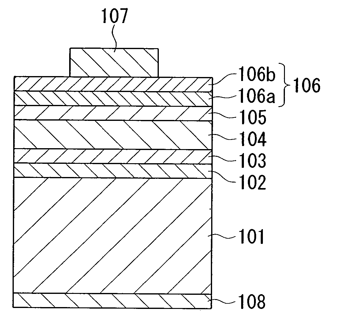
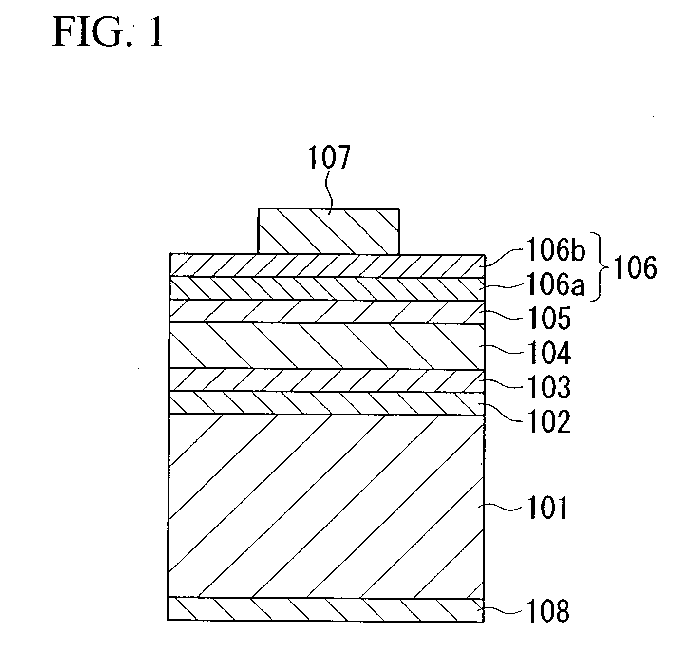
[0070] As the boron phosphide-based compound semiconductor device of the present invention, a light-emitting diode (LED) having a pn-double heterojunction (DH) structure comprising a boron phosphide-based compound semiconductor layer consisting of an amorphous layer and a polycrystal layer vapor-grown on an Si single crystal substrate was produced. FIG. 1 schematically shows the cross-sectional structure of LED produced.

[0071] As the substrate 101, a phosphorus (P)-doped n-type (111)-Si single crystal substrate was used.

[0072] First, an undoped boron phosphide (BP) amorphous layer 102 was deposited on the (111)-surface of the substrate 101 by an atmospheric pressure (nearly atmospheric pressure) metal-organic vapor phase epitaxy (MOVPE) method. The boron phosphide amorphous layer 102 was deposited at 450° C. by using triethylborane ((C2H5)3B) as the boron source and phosphine (PH3) as the phosphorus source. The ratio (PH3 / (C2H5)3B; V / III ratio) of the concentration of phosphorus s...


PUM

PropertyMeasurementUnit
temperatureaaaaaaaaaa
band gapaaaaaaaaaa

Abstract

A boron phosphide-based compound semiconductor device with excellent device properties, comprising a boron phosphide-based compound semiconductor layer having a wide bandgap is provided. The boron phosphide-based compound semiconductor layer consists of an amorphous layer and a polycrystal layer provided to join with the amorphous layer, and the room-temperature bandgap of the boron phosphide-based compound semiconductor layer is from 3.0 eV to less than 4.2 eV.

Description

CROSS-REFERENCE TO RELATED APPLICATIONS [0001] This application claims the benefit pursuant to 35 U.S.C. §119(e)(1) of U.S. Provisional Application, No. 60 / 432,249 filed Dec. 11, 2002.TECHNICAL FIELD [0002] The present invention relates to a boron phosphide-based compound semiconductor device comprising a boron phosphide-based compound semiconductor layer having a wide bandgap at room temperature and also relates to a production method thereof and a light-emitting diode. BACKGROUND ART [0003] Group-III nitride semiconductors such as gallium nitride (GaN) have been conventionally used for fabricating a nitride semiconductor device such as light-emitting diode (LED) or laser diode (LD) (see, for example, Non-Patent Document 1). The Group-III nitride semiconductor is known to have a relatively wide bandgap at room temperature and, for example, the room-temperature band gap of gallium nitride and aluminum nitride (AlN) having a hexagonal wurtzite structure is as large as 3.4 eV and 5.9 ...

Claims


Application Information

Patent Timeline
Patent Type & Authority Applications(United States)
IPC IPC(8): H01L29/82H01L21/205H01L29/20H01L29/205H01L33/12H01L33/14H01L33/16H01L33/30H01L33/32
CPCH01L29/2003H01L29/2006H01L29/205H01L33/12H01L33/14H01L33/16H01L21/0262H01L33/32H01L21/0237H01L21/02461H01L21/02502H01L21/0254H01L33/30
Inventor UDAGAWA, TAKASHI
Owner SHOWA DENKO KK
Why Eureka
Try Eureka