
Bipolar transistor with extrinsic stress layer

a technology of extrinsic stress and bipolar transistor, which is applied in the direction of transistors, semiconductor devices, electrical equipment, etc., can solve the problems of limited performance of bipolar devices, unexplored field of bipolar devices, and low field mobility of external strain devices, so as to improve performance and improve hole mobility. , the effect of improving the mobility of the field

Active Publication Date: 2006-03-02
GLOBALFOUNDRIES US INC
View PDF7 Cites 42 Cited by
  • Summary
  • Abstract
  • Description
  • Claims
  • Application Information

AI Technical Summary

Benefits of technology

[0014] Circuits benefit from ever increasing performance of the transistors. As mentioned above, MOSFET devices are finding increased performance from strained silicon lattice, which improves low field carrier mobility and thus the drive current in those devices. However, to the inventors' knowledge, external strain has not yet been engineered into bipolar devices for increased performance. Wherein there are many methods so far described to impart strain into MOSFET devices, this field is largely unexplored for bipolar devices.
[0015] Bipolar device (BJT) performance is partly limited by carrier transit time through the space-charge regions and through the neutral base. Low field mobility and saturation velocity enhancements will benefit this transit time. The performance is also limited by extrinsic resistances in the base, emitter and collector regions. These resistance values are dominated by low field electron and hole mobility and will be affected by strain in the device. Compressive strain will benefit hole mobility, and tensile strain will benefit electron mobility. Applied in the correct locations in the device, strain will significantly improve performance.
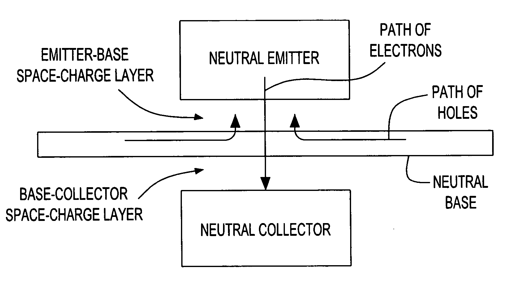
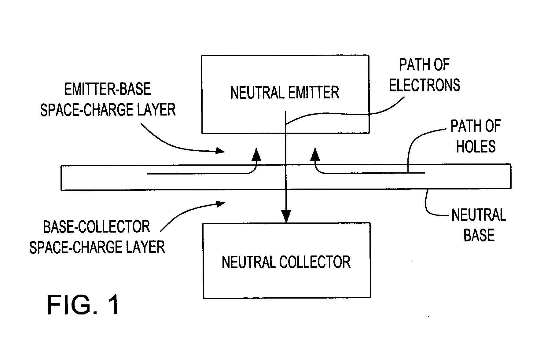
[0016] Referring to FIG. 1, the performance of an npn transistor could benefit from improving hole mobility in the lateral direction and improving electron mobility in vertical direction. In the opposite polarity case, a pnp transistor could benefit from improving electron mobility in the lateral direction and improving hole mobility in vertical direction.
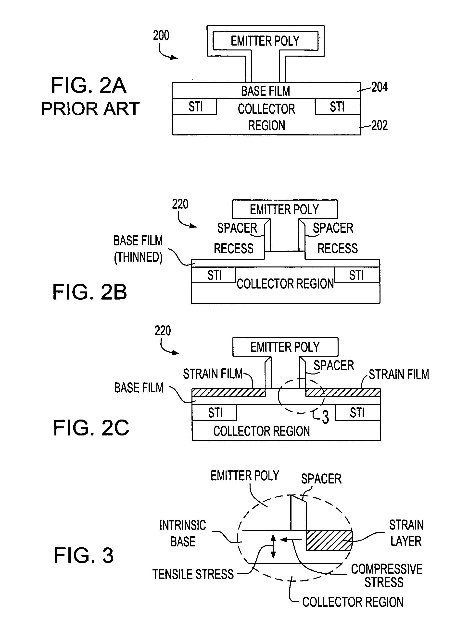
[0018] According to the invention, for an npn bipolar device tensile strain is applied to the intrinsic portion of the device (including the emitter, base and collector) in the direction of electron flow (vertical in the diagrams), and compressive strain is applied in the direction of hole flow (lateral in the diagrams), because holes flow principally in this direction within the base layers and improved hole mobility with compressive strain beneficially affects the resistance of the base terminal.

Problems solved by technology

However, to the inventors' knowledge, external strain has not yet been engineered into bipolar devices for increased performance.
Wherein there are many methods so far described to impart strain into MOSFET devices, this field is largely unexplored for bipolar devices.
Bipolar device (BJT) performance is partly limited by carrier transit time through the space-charge regions and through the neutral base.
The performance is also limited by extrinsic resistances in the base, emitter and collector regions.

Method used


Image

  • Bipolar transistor with extrinsic stress layer
  • Bipolar transistor with extrinsic stress layer
  • Bipolar transistor with extrinsic stress layer

Examples


Embodiment Construction

[0037] In the description that follows, numerous details are set forth in order to provide a thorough understanding of the present invention. It will be appreciated by those skilled in the art that variations of these specific details are possible while still achieving the results of the present invention. However, well-known processing steps may not be described in detail in order to avoid unnecessarily obfuscating the description of the present invention.

[0038] Materials (e.g., silicon dioxide) may be referred to by their formal and / or common names, as well as by their chemical formula. Regarding chemical formulas, numbers may be presented in normal font rather than as subscripts. For example, silicon dioxide may be referred to simply as “oxide”, chemical formula SiO2. For example, silicon nitride (stoichiometrically Si3N4, often abbreviated as “SiN”) may be referred to simply as “nitride”.

[0039] In the description that follows, exemplary dimensions may be presented for an illus...


PUM


Abstract

A method of increasing mobility of charge carriers in a bipolar device comprises the steps of: creating compressive strain in the device to increase mobility of holes in an intrinsic base of the device; and creating tensile strain in the device to increase mobility of electrons in the intrinsic base of the device. The compressive and tensile strains are created by forming a stress layer in close proximity to the intrinsic base of the device. The stress layer is at least partially embedded in a base layer of the device, adjacent an emitter structure of the device. The stress layer has different lattice constant than the intrinsic base. Method and apparatus are described.

Description

BACKGROUND OF THE INVENTION [0001] The invention relates to semiconductor device fabrication and, more particularly, to techniques for enhancing the performance of bipolar devices. [0002] A bipolar device is a semiconductor device, the operation of which is based on the use of both majority and minority carriers (also referred to as “charge carriers”). The majority and minority carriers are either electrons or holes, depending on the polarity of the device. [0003] An example of a bipolar device is the bipolar junction transistor (BJT) which is a transistor having three semiconductor regions referred to as emitter, base and collector. The emitter is a very high conductivity region which acts as a source of free carriers which are injected into the adjacent base region. The collector is a region which collects carriers from the base. The base region is sandwiched between the emitter and collector regions and generally controls the flow of free carriers between the emitter and the coll...

Claims


Application Information

Patent Timeline
Patent Type & Authority Applications(United States)
IPC IPC(8): H01L27/082
CPCH01L21/8249H01L29/7378H01L29/66242H01L29/242
Inventor CHIDAMBARRAO, DURESETIFREEMAN, GREGORY G.KHATER, MARWAN H.
Owner GLOBALFOUNDRIES US INC
Learn More