

Pattern matching apparatus and scanning electron microscope using the same
a scanning electron microscope and matching technology, applied in image enhancement, instruments, image data processing, etc., can solve the problems of reducing the efficiency of the inspection process, affecting the accuracy of the sem image, so as to achieve accurate isolation of the noise contained in the sem imag
- Summary
- Abstract
- Description
- Claims
- Application Information
AI Technical Summary
Benefits of technology
Problems solved by technology
Method used
Image

Examples
embodiment 1
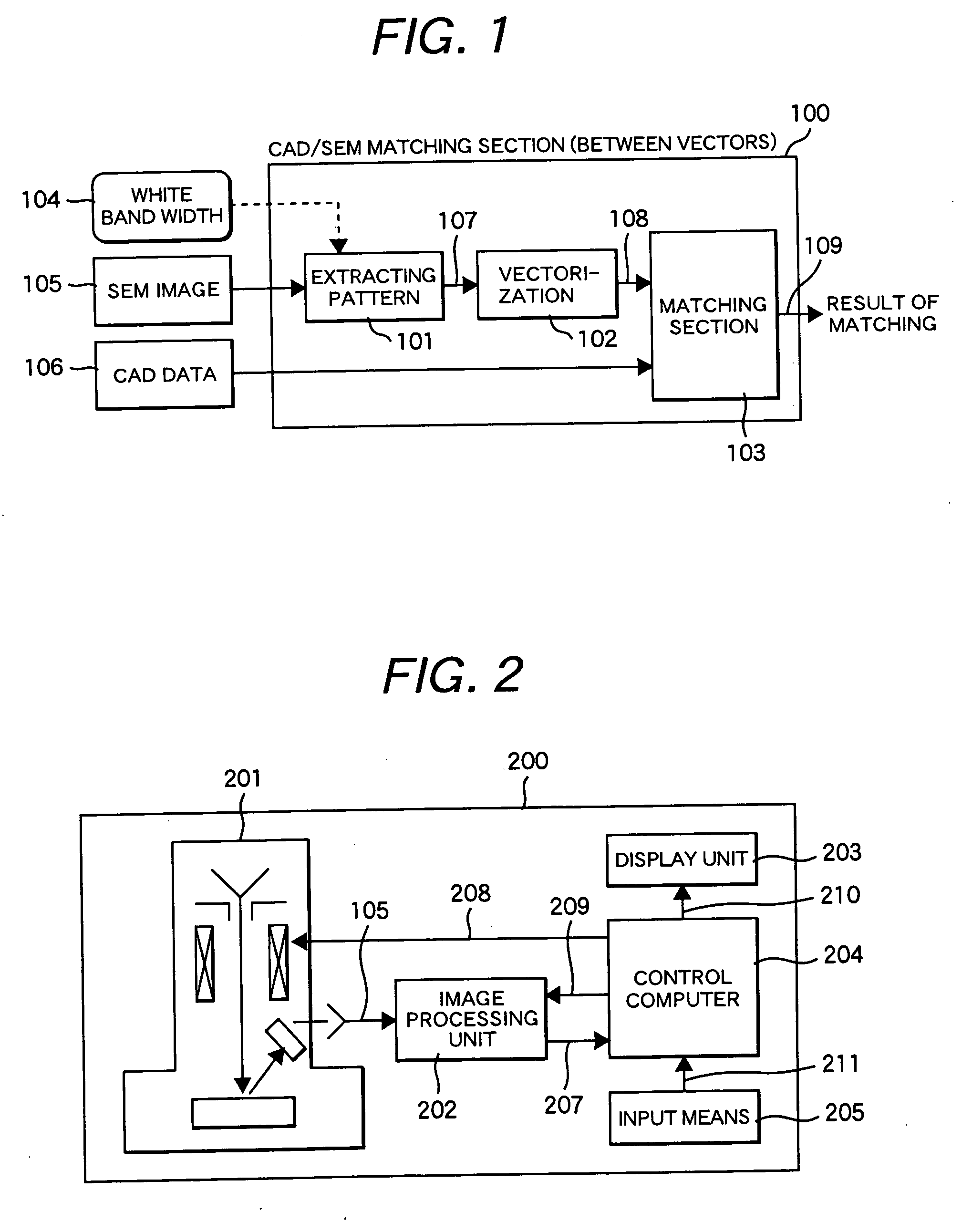
[0072]FIG. 2 shows the configuration of the scanning electron microscope system 200 in which the pattern matching apparatus 100 according to the present invention is applied to an image processing unit 202.
[0073] The scanning electron microscope system 200 comprises the SEM 201 which photographs an image of the semiconductor device; an image processing unit 202 which reduces SEM-specific noise contained in the SEM image 105 and executes the pattern matching process of the present invention; a control computer 204 for controlling the SEM 201 and the image processing unit 202; an input means 205 for inputting control data 211 used for controlling the scanning electron microscope system 200; and a display unit 203 which displays the n image photographed with the SEM 201, image processing results and indication data 210 for controlling the scanning electron microscope system 200.
[0074] Hereafter, each of the units that make up the system will be explained.
[0075] The control computer ...
embodiment 2
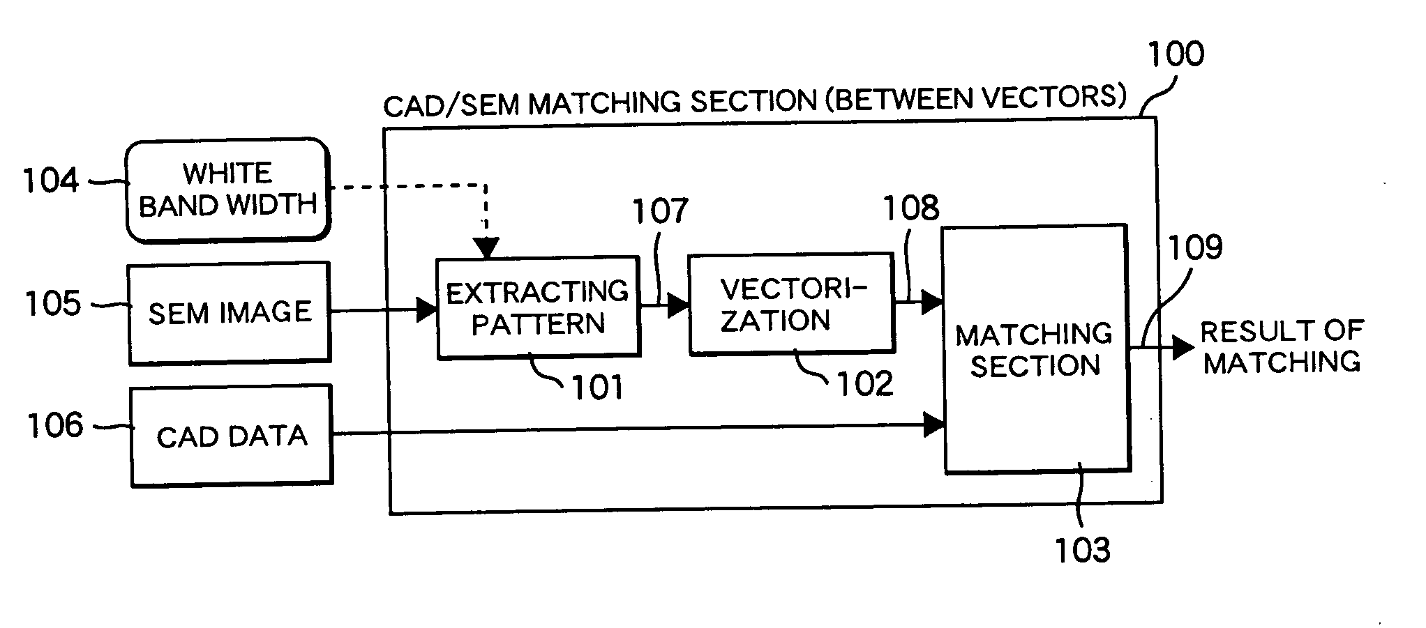
[0139] Furthermore, the objective of the pattern matching apparatus according to the present invention can be achieved by the configuration in which line information on the CAD data 106 is converted into an image as shown in FIG. 15 and then the images are matched.
[0140] A pattern matching apparatus 1500 according to the present invention comprises a pattern extracting section 101 which extracts a pattern image 107 from the SEM image 105 by using information 104 about the white band width; an image forming section 150 which creates image data 1503 from the CAD data 106; and a matching section 1502 which conducts the pattern matching of a pattern image 107 extracted from the SEM image 105 with image data 1503 of the CAD data 106, and outputs the result of the matching process 1504. In the same manner as in embodiment 1, the pattern matching apparatus 1500 can be included in an image processing unit 202 of a scanning electron microscope system 200. Moreover, the pattern matching appa...
embodiment 3
[0146] Furthermore, a pattern matching apparatus according to the present invention can be included in an independent environment which is different from a scanning electron microscope system as shown in embodiments 1 and 2. That is, it can be installed in a computer 1601 into which an image photographed by a SEM 201 shown in FIG. 16 is inputted via a local area network or by means of an externally connected memory. The computer 1601 is an information processing unit typified by a personal computer or a workstation. It comprises a signal input / output IF for inputting data into and outputting data from a scanning electron microscope system 1602 and other computers via a network or an externally connected memory; a memory for storing an SEM image, CAD data, programs for conducting pattern matching, and the results of the matching process; a CPU for executing the programs and creating the results of the matching process: a display unit 1603 for displaying screens for setting parameters...
PUM
 Abstract
Description
Claims
Application Information