
Method for manufacturing a quantum-dot element

a manufacturing method and quantum-dot technology, applied in the direction of manufacturing tools, superimposed coating process, chemical coating, etc., can solve the problems of nano-particulate process not being carried out in a continuous process, deterioration of quantum-dot element performance, and inability to manufacture photoelectric elements with nano-particulates. achieve the effect of avoiding quality loss due to transferring between different apparatuses and improving light, electricity and magnetism performan

Active Publication Date: 2006-03-02
IND TECH RES INST
View PDF4 Cites 29 Cited by
  • Summary
  • Abstract
  • Description
  • Claims
  • Application Information

AI Technical Summary

Benefits of technology

[0007] The object of the present invention is to provide a method for manufacturing a quantum-dot element so that the quantum dots can be distributed uniformly, the sizes of quantum dots can lie in the nano-order, and the performance of the quantum-dot element in light, electricity, and magnetismcan be improved. Furthermore, the electrode layer, the emitting material layer, and the carrier transport layer of the quantum-dot element can all be formed in the same apparatus, and thus the quality loss due to transferring between different apparatuses can be substantially avoided.
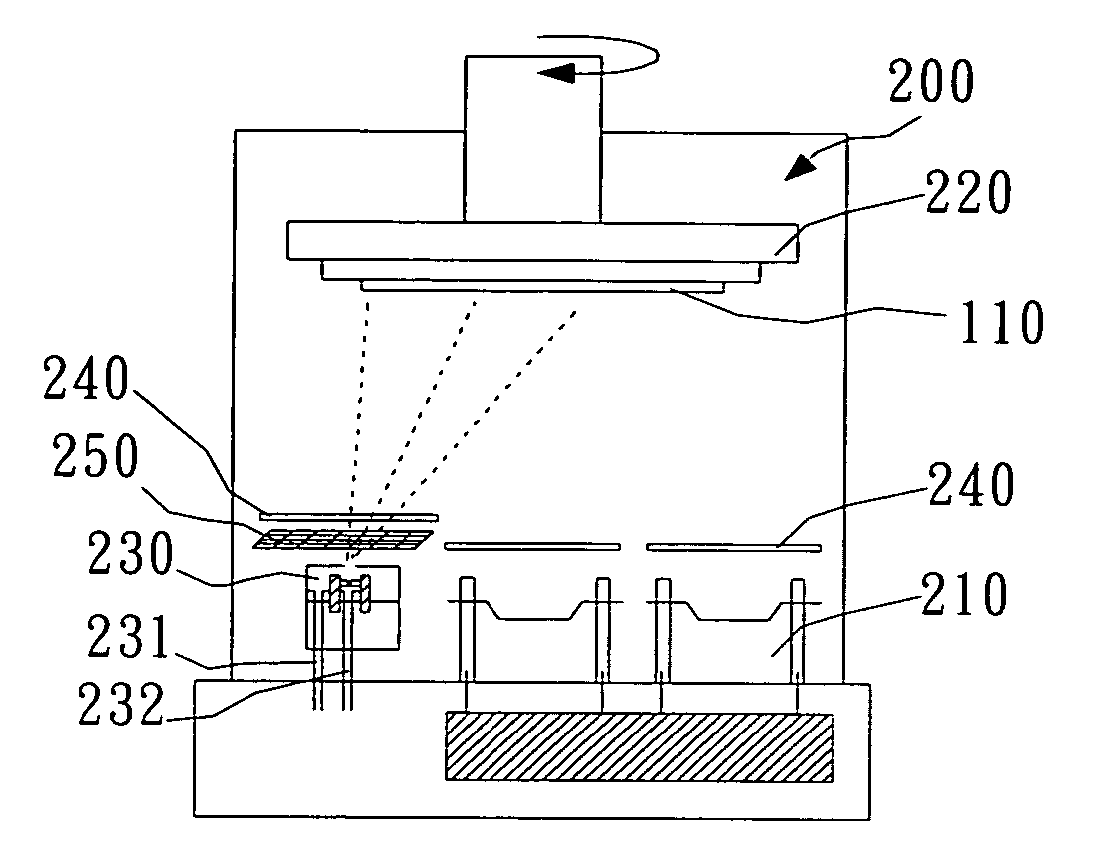
[0011] When the method of the present invention is carried out, the substrate with or without the bottom electrode layer is fixed on the substrate-supporting base in the deposition chamber first. Subsequently, the buffer layer or the electrode layer is formed by the vacuum deposition process, for example, the Chemical Vapor Deposition (CVD) process, or the Physical Vapor Deposition (PVD) process such as evaporation or sputtering. Therefore, the deposition chamber could be a CVD chamber, an evaporation chamber, or a sputtering chamber. Afterwards, a sample solution is prepared by considering the size of the droplet sprayed out from the atomizer, the property of the solvent, and the volume of the functionalized quantum dot according to the method of the present invention. Owing to the functionalized group, the quantum dots can be dispersed in the solvent uniformly. Thereafter, the sample solution is sprayed onto the surface of the substrate by the atomizer to form a quantum-dot layer. Moreover, the quantum dot can be a metal quantum dot, a semiconductor quantum dot, a magnetic quantum dot, an organic molecule quantum dot, or a polymer quantum dot. In addition, the diameter of the quantum dot formed by the present invention is less than 100 nm, and preferably ranges from several nano-meters to tens of nano-meters. The dispersion medium of the quantum dots, i.e. the solvent, can be water, an aqueous solution containing a surface-active agent, a polar organic solvent such as methanol, a non-polar organic solvent such as toluene, or a polymer solvent such as a diluted solution of a conjugate polymer, an epoxy resin, polymethylmethacrylate, polycarbonate, or a cyclic olefin co-polymer. The type of the atomizer is not restricted, and can be the conventional atomizer that sprays droplets by mixing and pressurizing the gas with the solution, or the supersonic atomizer that produces droplets by using the vibration energy of the piezoelectric ceramics. Besides, the substrate-supporting base is preferably a rotary plate that can drive the substrate to rotate and heat the substrate. More preferably, the substrate support base can adjust the rotation speed and the temperature of the substrate. Preferably, one shutter is mounted between the substrate supporting base and the atomizer, and the other shutter is mounted between the substrate supporting base and the evaporation or sputtering source for preventing the unstable evaporation or sputtering source from depositing on the substrate at the beginning of the heating of the evaporation or sputtering source. Similarly, at the initial stage of the spraying of the sample solution, the droplets are not uniform enough. Therefore, the shutter is also used for blocking the non-uniform droplets from arriving at the substrate.

Problems solved by technology

Although the nano-particulate as well as the composite of the nano-particulate and the organic molecule inherently has good material property, they become deteriorated when being applied to the photoelectric devices.
The main problem lies in that the manufacturing process of the nano-particulate is not compatible with the vacuum process for manufacturing the photoelectric element and, therefore, the manufacturing of the photoelectric element with the nano-particulates can not be carried out in a continuous process.
However, the quantum dots formed by these vacuum processes usually have too large particle sizes (usually larger than 10 nm) and too low densities.
Also, the particle sizes are not uniform enough.
Therefore, the quantum dots formed by the vacuum process are unsuitable for a manufacturing device with a large superficial content.
Besides, the product is easily contaminated during the mixing or the spin coating step, and consequently suffers from quality deterioration.
Moreover, the product might be damaged when it is transported between different manufacturing apparatuses.
However, although a uniform layer of quantum dots can be formed, the solvent might easily contaminate other parts of the quantum-dot element such as the carrier transport layer or the electrode.

Method used


Image

  • Method for manufacturing a quantum-dot element
  • Method for manufacturing a quantum-dot element
  • Method for manufacturing a quantum-dot element

Examples


embodiment 1

Preparation of the Sample Solution Containing CdSe / ZnS Quantum Dot with a Diameter of 3 nm

[0027] The sample solution is introduced by a piezoelectric atomizer to form toluene droplets with an average diameter of 1000 nm. If the influence to the diameter of the droplet caused by the CdSe / ZnS quantum dot is neglected and if each droplet is predetermined to have one quantum-dot particle, then the volume concentration of the sample solution can be calculated as the following equation (3):

(3 nm)3 / {(1000 nm)3+(3 nm)3}=9.00×10⁻⁹  (3)

[0028] If each droplet is predetermined to have three quantum-dot particles, then the desired concentration will be three times the concentration obtained from equation (3). Similarly, if each pair of droplets has only one quantum-dot particle, then the desired concentration will be half the concentration obtained from equation (3).

embodiment 2

Preparation of the Sample Solution Containing ZnO Particle with a Diameter of 1 μm

[0029] The sample solution is introduced by a conventional atomizer to form water droplets with an average diameter of 15 μm. If the influence to the diameter of the droplet caused by the ZnO particle is neglected and if each droplet is predetermined to have one particle, then the volume concentration of the sample solution can be calculated as the following equation (4):

(1 μm)3 / {(15 μm)3+(1 μm)3}=2.96×10⁻⁴  (4)

[0030] The volume concentration calculated from equation (4) equals to a weight concentration of 1.62×10⁻³.

[0031] If each droplet is predetermined to have five particles, then the desired concentration will be five times the concentration obtained from equation (4). Similarly, if each pair of droplets contains only one particle, then the desired concentration will be half the concentration obtained from equation (4).

embodiment 3

Preparation of the Sample Solution Containing Silica Nano-Particle with a Diameter of 20 nm

[0032] The sample solution is introduced by a piezoelectric atomizer to form water droplets with an average diameter of 100 nm. If the influence to the diameter of the droplet caused by the silica particle is neglected and if each droplet is predetermined to have one particle, then the volume concentration of the sample solution can be calculated as the following equation (5):

(20 nm)3 / {(100 nm)3+(20 nm)3}=4.63×10−3=0.463V %  (5)

[0033] If each droplet is predetermined to have fifteen particles, then the desired concentration will be fifteen times the concentration obtained from equation (5). Similarly, if each pair of droplets contains only one particle, then the desired concentration will be half the concentration obtained from equation (5).


PUM

PropertyMeasurementUnit
diameteraaaaaaaaaa
particle sizesaaaaaaaaaa
diameteraaaaaaaaaa

Abstract

A method for manufacturing a quantum-dot element is disclosed. The method includes the following steps. First, a deposition chamber having at least one atomizer and a substrate-supporting base is provided. The atomizer is connected to a gas inlet and a sample inlet. Afterwards, a sample solution is prepared composed of a plurality of functionalized quantum dots dispersed in a solvent. Simultaneously, a substrate is placed on the substrate-supporting base in the deposition chamber. Finally, the sample solution and a gas are transferred into the atomizer through the sample inlet and the gas inlet respectively for generating quantum-dot droplets, which subsequently deposit on the substrate in the deposition chamber. The quantum-dot element manufactured by the present invention has a uniform distribution of quantum dots that have a small size and, therefore, the quality of the quantum-dot element can be substantially improved.

Description

BACKGROUND OF THE INVENTION [0001] 1. Field of the Invention [0002] The present invention relates to a method for manufacturing a quantum-dot element and, more particularly, to a method for manufacturing a photoelectric element with colloidal quantum dots, such as a light-emitting diode, a laser diode, a detector, a photonic crystal, or a magnetic thin film. [0003] 2. Description of Related Art [0004] Recently, the hybrid of organic or inorganic materials has become the emphasis of the development in photoelectric materials. On the other hand, the nano-particulate obtained by liquid or gaseous synthesis is also the focus of the development in material technology. Although the nano-particulate as well as the composite of the nano-particulate and the organic molecule inherently has good material property, they become deteriorated when being applied to the photoelectric devices. The main problem lies in that the manufacturing process of the nano-particulate is not compatible with the v...

Claims


Application Information

Patent Timeline
Patent Type & Authority Applications(United States)
IPC IPC(8): H01L21/00
CPCB82Y10/00H01L33/08H01L29/0673H01L29/0665
Inventor CHEN, HSUEH-SHIHLO, DAI-LUONCHANG, GWO-YANGCHEN, CHIEN-MING
Owner IND TECH RES INST
Learn More