

Semiconductor device
- Summary
- Abstract
- Description
- Claims
- Application Information
AI Technical Summary
Benefits of technology
Problems solved by technology
Method used
Image

Examples
embodiment 1
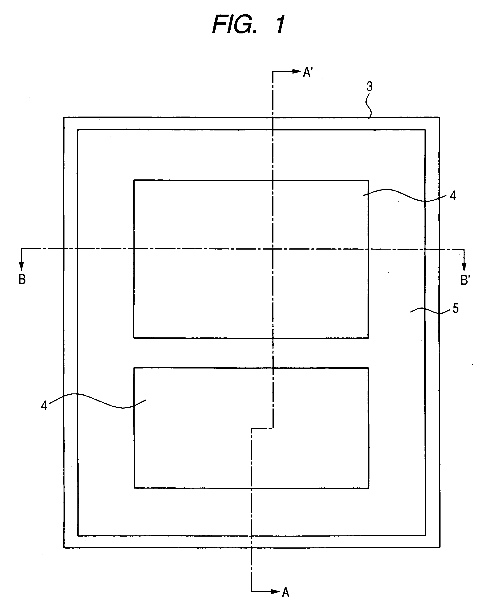
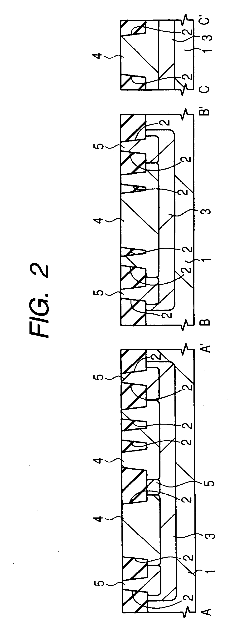
[0048] The semiconductor device according to Embodiment 1 has a nonvolatile memory. The manufacturing steps of the semiconductor device of Embodiment 1 will next be described with reference to FIGS. 1 to 13.
[0049]FIGS. 1, 3, 6 and 11 are each a fragmentary plan view of a memory cell region of the semiconductor device of Embodiment 1 during its manufacturing step, while FIGS. 2, 4, 5, 7-10, 12 and 13 are each a fragmentary cross-sectional view illustrating the manufacturing step of the semiconductor device of Embodiment 1. In each cross-sectional view, a portion marked with A and A′ is a cross-section taken along a line A-A′ in the corresponding plan view; a portion marked with B and B′ is a cross-section taken along a line B-B′ in the corresponding plan view, and a portion marked with C and C′ is a cross-section of a part (a region in which an n channel type MISFET (Metal Insulator Semiconductor Field Effect Transistor) is to be formed) of a peripheral circuit region. Each plan vie...
embodiment 2
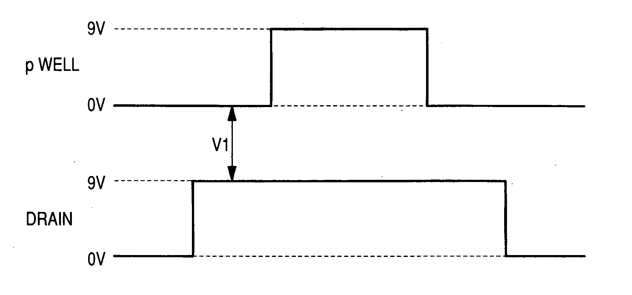
[0078] Writing, erasing and reading operations in a nonvolatile memory according to Embodiment 2 will next be described with reference to FIG. 18.
[0079]FIG. 18 illustrates a cross-section taken along a line D-D′ of FIG. 14 in Embodiment 1. As illustrated in FIG. 18, the nonvolatile memory of Embodiment 2 has almost a similar structure to that of the nonvolatile memory according to Embodiment 1.
[0080] The writing and reading operations of data in the nonvolatile memory of Embodiment 2 are similar to those of the nonvolatile memory of Embodiment 1. As illustrated in FIG. 18, erasing of data is carried out by applying 9V to the n well 5 (n type semiconductor isolation region 3), 0V is applied to the p type semiconductor regions 15B (the p wells 4 having MISFETs Qw1, Qw2, Qr1, Qr2 formed thereover), −9V to the p type semiconductor regions 15A (the p wells 4 having the capacitive elements C1, C2 formed thereover), and 7V to the drain (n type semiconductor region 14B) of the data writin...
embodiment 3
[0083] Data writing, erasing and reading operations in a nonvolatile memory according to Embodiment 3 will next be described with reference to FIG. 19.
[0084]FIG. 19 illustrates the cross-section taken along a line D-D′ of FIG. 14 in Embodiment 1. As illustrated in FIG. 19, the nonvolatile memory of Embodiment 3 has almost a similar structure to that of the nonvolatile memory of Embodiment 1.
[0085] The data erasing and reading operations in the nonvolatile memory of Embodiment 3 are similar to those of the nonvolatile memory of Embodiment 1. As illustrated in FIG. 19, writing of data is carried out by applying 9V to the n well 5 (n type semiconductor isolation region 3), −9V to the p type semiconductor regions 15B (the p wells 4 having the MISFETs Qw1, Qw2, Qr1, Qr2 formed thereover), and 9V to the p type semiconductor regions 15A (the p wells 4 having the capacitive elements C1, C2 formed thereover), and setting the source and drain (n type semiconductor regions 14B) of the data w...
PUM
 Abstract
Description
Claims
Application Information