

Plasma processing apparatus and method
a processing apparatus and plasma technology, applied in the direction of coatings, electric discharge lamps, electric lighting sources, etc., can solve the problems of poor plasma resistance properties, etching surface roughness, vertical lines (striation), etc., to achieve high selectivity etching, effective prevention of deposition, and high rate etching
- Summary
- Abstract
- Description
- Claims
- Application Information
AI Technical Summary
Benefits of technology
Problems solved by technology
Method used
Image

Examples
embodiment 1
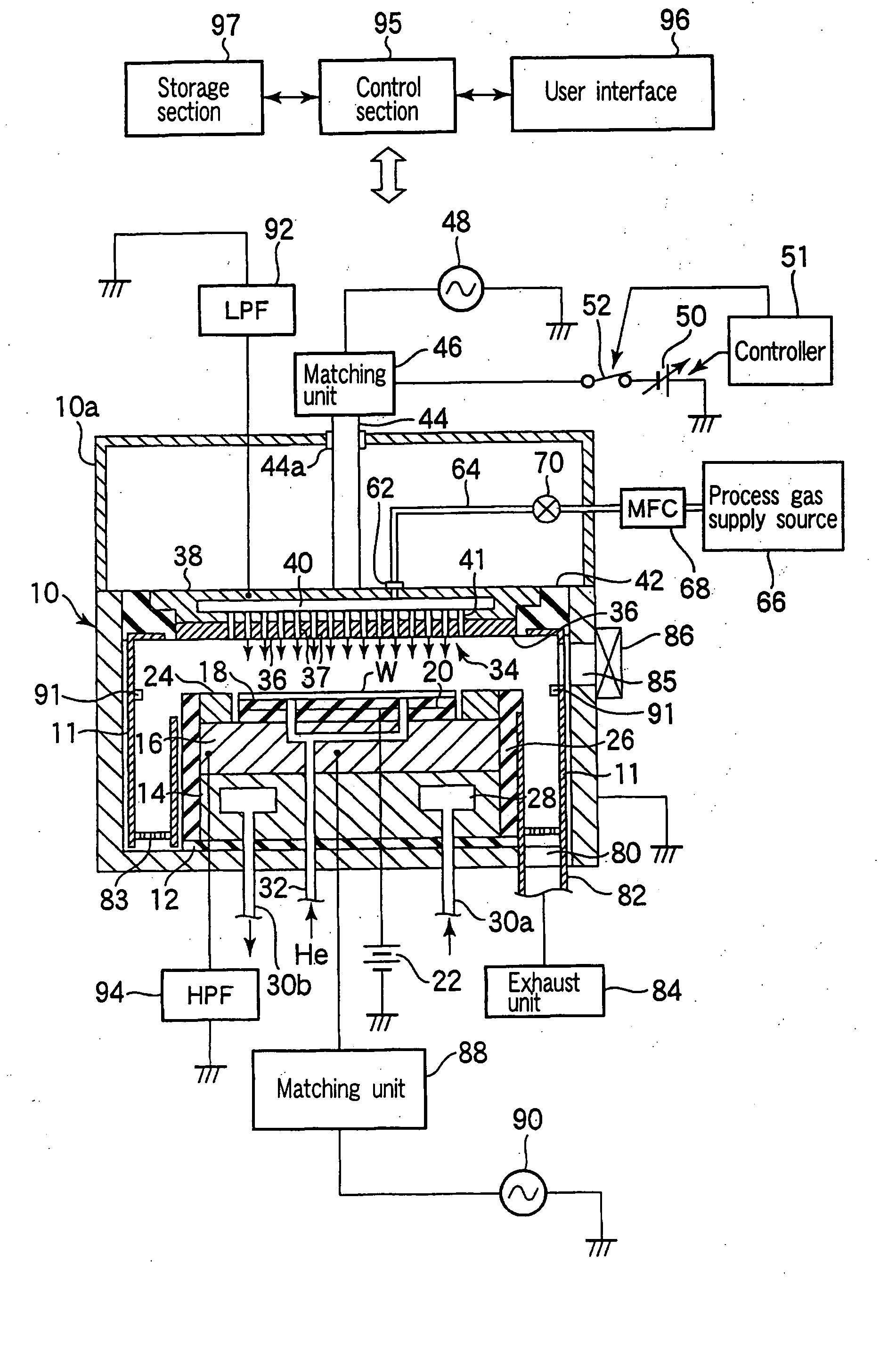
[0133] An embodiment 1 will be explained first. FIG. 1 is a sectional view schematically showing a plasma etching apparatus according to the embodiment 1 of the present invention.
[0134] This plasma etching apparatus is structured as a parallel-plate plasma etching apparatus of the capacitive coupling type. The apparatus includes a cylindrical chamber (process chamber) 10, which is made of, e.g., aluminum with an anodization-processed surface. The chamber 10 is protectively grounded.
[0135] A columnar susceptor pedestal 14 is disposed on the bottom of the chamber 10 through an insulating plate 12 made of, e.g., a ceramic. A susceptor 16 made of, e.g., aluminum is disposed on the susceptor pedestal 14. The susceptor 16 is used as a lower electrode, on which a target substrate, such as a semiconductor wafer W, is placed.
[0136] The susceptor 16 is provided with an electrostatic chuck 18 on the top, for holding the semiconductor wafer W by an electrostatic attraction force. The electro...
embodiment 2
[0271] Next, an explanation will be given of an embodiment 2 of the present invention.
[0272]FIG. 34 is a sectional view schematically showing a plasma etching apparatus according to an embodiment 2 of the present invention. In FIG. 34, the constituent elements the same as those shown in FIG. 1 are denoted by the same reference symbols, and a repetitive description thereon will be omitted.
[0273] In place of the upper electrode 34 of the embodiment 1, this embodiment includes an upper electrode 34′ having the following structure. Specifically, the upper electrode 34′ comprises an outer upper electrode 34a and an inner upper electrode 34b. The outer upper electrode 34a has a ring shape or doughnut shape and is disposed to face a susceptor 16 at a predetermined distance. The inner upper electrode 34b has a circular plate shape and is disposed radially inside the outer upper electrode 34a while being insulated therefrom. In terms of plasma generation, the outer upper electrode 34a main...
embodiment 3
[0313] Next, an explanation will be given of an embodiment 3 of the present invention.
[0314] In the embodiment 3, the constituent elements common to those of the embodiments 1 and 2 are denoted by the same reference symbols.
[0315]FIG. 40 is a sectional view schematically showing a plasma etching apparatus according to the embodiment 3 of the present invention.
[0316] This plasma etching apparatus is of the type that applies two RF powers with different frequencies to the lower side. Specifically, a radio frequency (RF) power with, e.g., 40 MHz for plasma generation from a first RF power supply 88 and a radio frequency (RF) with, e.g., 2 MHz for ion attraction from a second RF power supply 90 are applied to a lower electrode or susceptor 16. Further, as shown in FIG. 40, a variable DC power supply 50 is connected to an upper electrode 34 to apply a predetermined direct current (DC) voltage. With reference to FIG. 41, this plasma etching apparatus will be explained in more detail.
[...
PUM
| Property | Measurement | Unit |
|---|---|---|
| dielectric constant | aaaaa | aaaaa |
| dielectric constant | aaaaa | aaaaa |
| frequency | aaaaa | aaaaa |
Abstract
Description
Claims
Application Information