Organic light-emitting device
a light-emitting device and organic technology, applied in the direction of organic semiconductor devices, discharge tubes/lamp details, natural mineral layered products, etc., can solve the problems of durability and deterioration due, and achieve the effects of high luminance, long life and high purity
- Summary
- Abstract
- Description
- Claims
- Application Information
AI Technical Summary
Benefits of technology
Problems solved by technology
Method used
Image

Examples
example 1
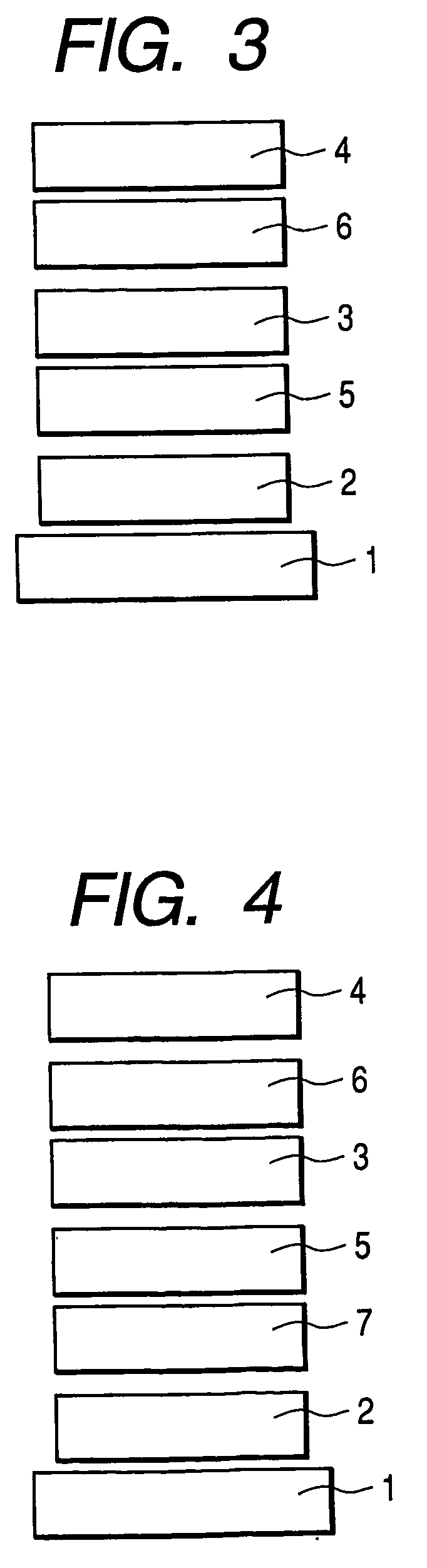
[0066] An organic light-emitting device having the structure shown in FIG. 3 was prepared in a method illustrated below.
[0067] On a glass substrate as substrate 1, indium tin oxide (ITO) of 120 nm in thickness as anode 2 was deposited by a sputtering process and ultrasonically cleaned with acetone and isopropyl alcohol (IPA) in this order, and dried by boiling with IPA after the cleaning. Further, it was cleaned with UV / ozone. The resultant structure is referred to a transparent conductive supporting substrate.
[0068] There was prepared a 0.5% by weight chloroform solution of the compound represented by the following structural formula:
[0069] The solution was dropped on the ITO electrode (anode 2) of the transparent conductive supporting substrate, and was subjected to a spin coating first at a revolution of 500 RPM for 10 seconds and then at a revolution of 1,000 RPM for one minute to form a film. It was dried in a vacuum oven at 80° C. for 10 minutes to completely remove the so...
examples 2 to 7
[0074] Devices were prepared and evaluated in the same manner as in Example 1-except that illustrated compounds shown in Table 6 replaced the illustrated compound [1]-6. The results are shown in Table 6.
TABLE 6IllustratedAppliedMaximumcompoundvoltageLuminanceluminanceEfficiencyExampleNo.(V)(cd / m2)(cd / m2)(lm / W)2[1]-349167052000.603[1]-418184061500.654[1]-469173054800.605[1]-579205069900.676[1]-648220072700.727[1]-668260077000.85
example 8
[0075] A device was prepared in the same manner as in Example 1 except that the above illustrated compound No. [1]-41 and the above illustrated compound No. [2]15 (weight ratio of 5:100) replaced the above illustrated compound No. [1]-6 and the above illustrated compound No. [2]-1 respectively to be subjected to the co-deposition to provide light-emitting layer 3 of 20 nm.
[0076] When the obtained device was applied with a direct-current voltage of 9 V using an ITO electrode (anode 2) as a positive electrode and an Al—Li electrode (cathode 4) as a negative electrode, the emission of blue light having an emission luminance of 1,680 cd / m2, a maximum luminance of 4,650 cd / m2 and a luminous efficiency of 0.57 lm / W was observed.
PUM
| Property | Measurement | Unit |
|---|---|---|
| Electric potential / voltage | aaaaa | aaaaa |
| Electric potential / voltage | aaaaa | aaaaa |
| Luminous efficiency | aaaaa | aaaaa |
Abstract
Description
Claims
Application Information
 - Generate Ideas
- Intellectual Property
- Life Sciences
- Materials
- Tech Scout
- Unparalleled Data Quality
- Higher Quality Content
- 60% Fewer Hallucinations
Browse by: Latest US Patents, China's latest patents, Technical Efficacy Thesaurus, Application Domain, Technology Topic, Popular Technical Reports.
© 2025 PatSnap. All rights reserved.Legal|Privacy policy|Modern Slavery Act Transparency Statement|Sitemap|About US| Contact US: help@patsnap.com