Method of forming fine particle array on substrate and semiconductor element

a technology of fine particles and substrates, applied in nanoinformatics, manufacturing tools, oxygen/ozone/oxide/hydroxide, etc., can solve problems such as difficulties in fulfilling a desired function, and achieve the effect of suppressing the reoxidation of reduced fine particles

Active Publication Date: 2006-04-06
PANASONIC CORP
View PDF3 Cites 12 Cited by
  • Summary
  • Abstract
  • Description
  • Claims
  • Application Information

AI Technical Summary

Benefits of technology

[0025] In the method of arranging fine particles on a substrate, inorganic metal oxide fine particles are arranged on a substrate in the oxidized state which is stable having a high melting point and a high oxidation number; an insulating layer is produced thereon; and thereafter, reduction is executed into the metal or the oxide having a lower oxidation number (semiconductor or the like). Accordingly, an effect of preventing deterioration, movement and aggregation of the cores may be exerted, contrary to the conventional techniques which produce an insulating layer on metal cores or semiconductor cores having a low melting point and being unstable.
[0026] Also, in the method of arranging fine particles on a substrate according to the present invention, the inorganic metal oxide is reduced following the production of the insulating layer, therefore, an effect of decreasing damage (defect) in reduction, which was generated on the inorganic metal oxide fine particles (core) in formation of the insulating layer may be also exerted.
[0028] According to the method of forming a fine particle array of the present invention, suppression of reoxidization of reduced fine particles is enabled.

Problems solved by technology

However, the constitution according to the aforementioned conventional techniques involved problems of reoxidation of the metal atom aggregate produced by the reduction treatment due to exposure to the atmospheric air, or in the initial stage of laminating an insulating layer in the following step.
Hence, majority of the embedded fine particles return back to the original metal oxide to result in difficulties in fulfilling a desired function.

Method used


Image

  • Method of forming fine particle array on substrate and semiconductor element
  • Method of forming fine particle array on substrate and semiconductor element
  • Method of forming fine particle array on substrate and semiconductor element

Examples


embodiment 1

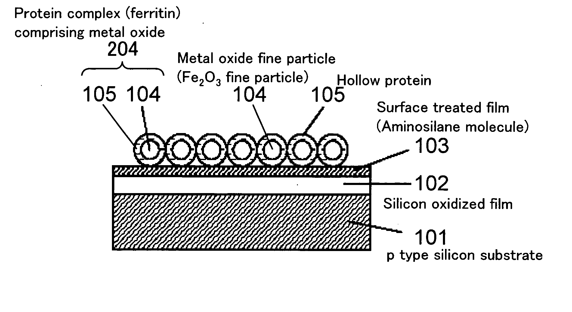
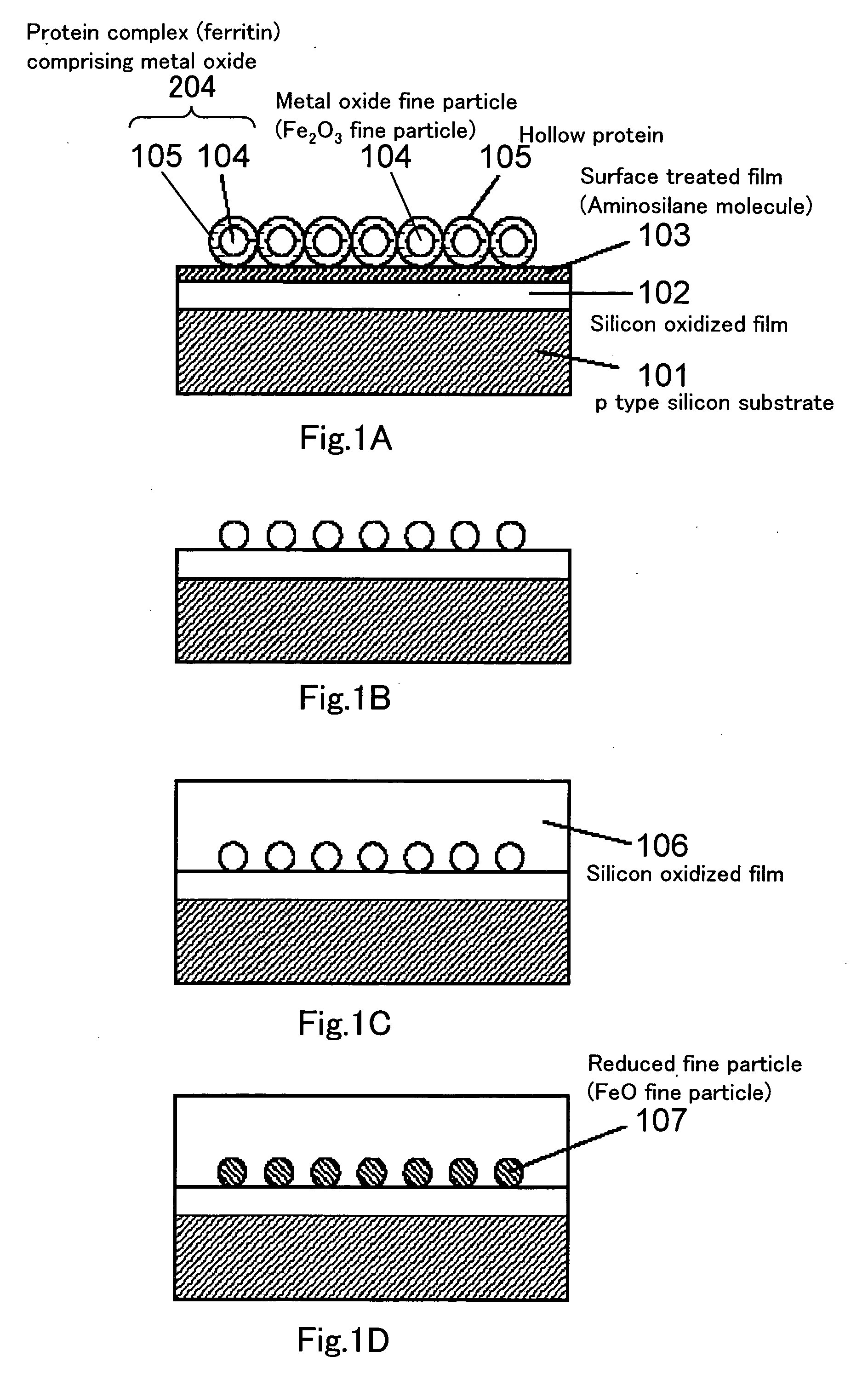
[0043] A method of forming a fine particle array on a substrate according to Embodiment 1 of the present invention comprises, as shown in FIG. 1A to FIG. 1D, a step A of fixing metal oxide fine particles 104 and protein complexes (protein complex) 204 comprising a hollow protein 105, which includes the metal oxide fine particle 104 therein, on a substrate 101, a step B of removing the hollow protein 105 while leaving the metal oxide fine particles 104 on the substrate 101, a step C of laminating an insulating layer 106 to give a film thickness of 3 nm or greater and 100 nm or less, which is hardly reduced compared to the metal oxide fine particles 104, on the substrate 101 on which the metal oxide fine particles 104 were disposed, and a step D of reducing the metal oxide fine particles 104 by subjecting the substrate 101, on which the insulating layer 106 was laminated in the step C, to a heat treatment in a reducing atmosphere to yield reduced fine particles 107.

[0044] According t...

embodiment 2

[0084] In this Embodiment 2, one example of the method of forming a fine particle array in which a silicon nitride is used as an insulator will be illustrated.

[0085] In FIG. 6, cross sectional structure of the substrate produced in this Embodiment is shown. First, a p type silicon substrate 101 is washed to remove naturally oxidized film. Thereafter, a silicon thermally-oxidized film 102 having a film thickness of 3 nm was formed on the surface at 800° C. with a rapid thermal oxidation (RTO) method.

[0086] Next, thus produced substrate was subjected to a UV ozone treatment, and the contaminants (organic compounds and the like) adsorbed on the surface were removed to obtain a clean surface. In the UV ozone treatment, the substrate is exposed into an atmosphere of a mixture of ozone and oxygen under an ultraviolet irradiating condition to oxidize and remove the organic compound molecules. In this Embodiment, the treatment was conducted at 110° C. for 10 min. Because the substrate sur...

embodiment 3

[0100] This Embodiment 3 illustrates one example of a semiconductor element in which silicon oxide is used as an insulator.

[0101] Also in this Embodiment, a substrate having iron oxide cores embedded into an insulator was produced, and it was subjected to a reduction treatment, in a similar manner to Embodiment 2. However, silicon oxide (SiO2) was used instead of silicon nitride as an insulating layer into which the cores are embedded. Cross sectional structural drawing of the semiconductor element of this Embodiment is shown in FIG. 9.

[0102] Onto a substrate having iron oxide cores produced according to similar steps of Embodiment 1 was deposited a SiO2 insulating layer 106 by plasma CVD. In this step, deposition was carried out using a monosilane (SiH4) gas and a nitrous oxide (N2O) gas as sources of plasma CVD, and a nitrogen gas as a carrier, at a substrate temperature of 400° C., with RF power of 50 W for 60 sec. As a result, a SiO2 insulating layer 106 having a film thicknes...


PUM

PropertyMeasurementUnit
thicknessaaaaaaaaaa
thicknessaaaaaaaaaa
temperatureaaaaaaaaaa

Abstract

An object of the present invention is to provide a method of forming fine particles on a substrate in which reoxidization of reduced fine particles is suppressed. Reduced fine particles (FeO fine particles) are formed by embedding metal oxide fine particles (Fe2O3 fine particles) fixed on a p type silicon semiconductor substrate into a silicon oxidized film, and carrying out a heat treatment in a reducing gas atmosphere. Presence of the silicon oxidized film enables suppression of reoxidization of the reduced fine particles (FeO fine particles) due to exposure to the ambient air.

Description

[0001] This is a continuation application under U.S.C 111(a) of pending prior International application No. PCT / JP2005 / 009629, filed on May 26, 2005.BACKGROUND OF THE INVENTION [0002] 1. Field of the Invention [0003] The present invention relates a method of forming a fine particle array on a substrate utilizing a hollow protein. Further, the present invention relates to a semiconductor element utilizing the fine particle array. [0004] 2. Description of the Related Art [0005] There were conventional methods of forming fine particles which comprise fixing a protein complex, which can include a fine particle therein, on a substrate; removing the protein by a heat treatment or the like; and reducing in a reducing atmosphere to produce a metal atom aggregate (for example, see, Japanese Patent Provisional Publications No. 2002-223016, No. H11-45990 and No. H11-233752). [0006]FIG. 2 shows a conventional method of forming fine particles described in Japanese Patent Provisional Publications...

Claims


Application Information

Patent Timeline
Patent Type & Authority Applications(United States)
IPC IPC(8): B22F9/20B28B23/00H01L21/28H01L21/8247H01L27/115H01L29/06H01L29/423H01L29/788H01L29/792
CPCB82Y10/00H01L21/28273H01L21/28282H01L29/42332H01L29/40114H01L29/40117
Inventor YOSHII, SHIGEOUEDA, MICHIHITOMATSUKAWA, NOZOMUYAMASHITA, ICHIRO
Owner PANASONIC CORP
Why Eureka
Try Eureka