High electron mobility transistors with Sb-based channels

a high electron mobility, transistor technology, applied in the direction of semiconductor devices, basic electric elements, electrical apparatus, etc., can solve the problems of increasing the complexity of material growth and device design requirements, increasing the complexity of material growth and fabrication technology of antimony-based hemts, and being susceptible to significant charge control problems. to achieve the effect of increasing operating speeds

Inactive Publication Date: 2006-04-13
THE UNITED STATES OF AMERICA AS REPRESENTED BY THE SECRETARY OF THE NAVY
View PDF7 Cites 44 Cited by
  • Summary
  • Abstract
  • Description
  • Claims
  • Application Information

AI Technical Summary

Benefits of technology

[0008] It is an object of this invention to provide transistors that employ advanced material designs to increase operating speeds.

Problems solved by technology

Although improvements have been made in recent years, the material growth and fabrication technology for antimony-based HEMTs is relatively immature.
For the case of AlSb / InAs HEMTs, the high reactivity of AlSb in air and the low valence-band offset of the AlSb / InAs heterojunction increase the complexity of the material growth and device design requirements.
HEMTs with InAsySb1−y channels, however, are susceptible to significant charge control problems associated with impact ionization in the channel due to the narrow bandgaps of these materials.
These effects become increasingly pronounced as the gate length is reduced due to the higher fields present, thus hindering the high-frequency performance of short-gate length HEMTs and limiting their operating voltage range.

Method used


Image

  • High electron mobility transistors with Sb-based channels
  • High electron mobility transistors with Sb-based channels
  • High electron mobility transistors with Sb-based channels

Examples


Embodiment Construction

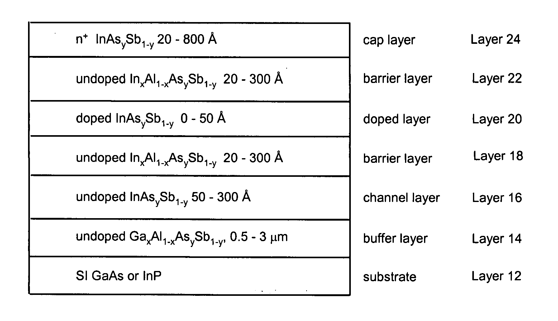
[0020] High electron mobility transistors of this invention employ advanced material layer designs that can increase operating speed to over 500 GHz and reduce power dissipation by a factor of at least two. The HEMTs utilize InxAl1−xAsySb1−y, InxAl1−xPySb1−y, or GaxAl1−xAsySb1−y for the barrier layer and InAsySb1−y in the channel. As a result, the devices exhibit improved frequency performance while operating at lower bias voltage.

[0021] More specifically, the HEMTs of this invention include, as shown in FIG. 1, a semi-insulating GaAs or InP substrate 12, buffer layer 14 of undoped InxAl1−xAsySb1−y, InxAl1−xPySb1−y, or GaxAl1−xAsySb−y disposed on the substrate, channel layer 16 through which electrons flow horizontally, as depicted in FIG. 1, of undoped InAsySb1−y disposed on the buffer layer, first barrier layer 18 of undoped InxAl1−xAsySb1−y, InxAl1−xPySb1−y, or GaxAl1−xAsySb1−y disposed on the channel layer, silicon or tellurium-doped layer 20 of InAsySb1−y, InxAl1−xAsySb1−y, In...


PUM


Abstract

This invention pertains to an electronic device containing a semi-insulating substrate, a buffer layer of an antimony-based material disposed on said substrate, a channel layer of InAsySb1−y material disposed on said buffer layer, a barrier layer of an antimony-based disposed on said channel layer, and a cap layer of InAsySb1−y material disposed on said barrier layer, wherein the device can have frequency of on the order of 500 GHz and a reduced power dissipation.

Description

CROSS REFERENCE TO RELATED APPLICATIONS [0001] This application claims the benefit of U.S Provisional Application No. 60 / 615,118 filed Sep. 30, 2004.BACKGROUND OF THE INVENTION [0002] 1. Field of the Invention [0003] This invention pertains to high electron mobility transistors (HEMTs) that employ advanced material designs. [0004] 2. Description of Related Art [0005] Future generations of microwave and millimeter-wave radar, communications, electronic warfare, smart weapons, and imaging systems will require higher precision, smaller size, increased bandwidth, lower operating voltages, and lower cost of production. To meet the demand for improved high-frequency performance, considerable effort within the last 10 years or so has focused on the development of gallium arsenide(GaAs)-based and indium phosphide(InP)-based HEMTs. As a result, a variety of HEMT analog and digital circuits have been fabricated which exhibit higher gain, efficiency, and switching speeds with lower power dissi...

Claims


Application Information

Patent Timeline
Patent Type & Authority Applications(United States)
IPC IPC(8): H01L29/739
CPCH01L29/7783
Inventor BOOS, JOHN BRADLEYBENNETT, BRIAN R.MAGNO, RICHARDTINKHAM, BRADPAPANICOLOU, NICHOLAS A.
Owner THE UNITED STATES OF AMERICA AS REPRESENTED BY THE SECRETARY OF THE NAVY
Why Eureka
Try Eureka