Porous low dielectric constant compositions and methods for making and using same

Active Publication Date: 2006-04-13
VERSUM MATERIALS US LLC
View PDF14 Cites 80 Cited by
  • Summary
  • Abstract
  • Description
  • Claims
  • Application Information

AI Technical Summary

Benefits of technology

[0004] A porous organosilicate glass (OSG) film consisting of a single phase of a material represented by the formula SivOwCxHyFz, where v+w+x+y+z=100%, v is from 10 to 35 atomic %, w is from 10

Problems solved by technology
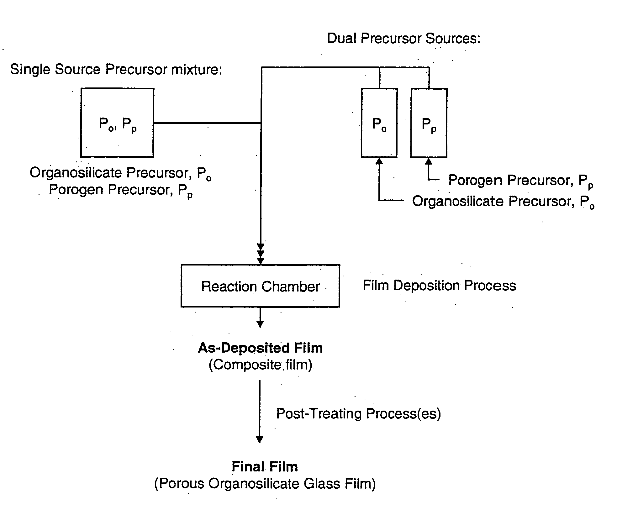
Unfortunately, many of these film properties suffer

Method used


Image

  • Porous low dielectric constant compositions and methods for making and using same
  • Porous low dielectric constant compositions and methods for making and using same
  • Porous low dielectric constant compositions and methods for making and using same

Examples


example 1

Variation of the Porogen Precursor to Silicon-Containing Precursor Stoichiometry

[0136] Composite films were deposited from a mixture of cyclohexanone (CHO) and diethoxymethylsilane (DEMS). The deposition conditions were as follows: the plasma power was 450 Watts, reaction chamber pressure was 8 torr, electrode spacing was 350 milli-inches, carrier gas was Helium at a flow rate of 210 sccm, and the substrate temperature was 225° C. The CHO and DEMS flow rates were varied to control the ratio of CHO and DEMS introduced into the reaction chamber, while leaving constant the overall flow rate of chemical into the chamber. The films were post-treated by exposing them to broadband UV light (λ=200-400 nm) under vacuum for 5 minutes.

TABLES 1a and 1bAs-deposited and final film properties, respectively, for films depositedusing cyclohexanone and DEMS.CHO flowDEMS flowTotal FlowCHO:DEMSDepositionRefractive Index(mg / min)(mg / min)(mg / min)ratioRate (nm / min)(As Dep'd)4501506004.102001.48040020060...

example 2

Porogen Precursor Functional Groups

[0138] The structure and / or composition of the porogen precursor may also be used to control the film properties. Composite films were deposited from CHO or 1,2,4-trimethylcyclohexane (TMC). Table 2 compares the neat liquid properties of these precursors. The CHO precursor consists of a 6 carbon ring with a ketone functional group, while the TMC precursor has a 6 carbon ring with three methyl groups attached at the 1, 2, and 4-positions.

TABLE 2Properties of neat liquid porogen precursors.H / CMolecularDensityRefractiveBoilingPorogen PrecursorFormularatioWeight(g / mL)IndexPoint (° C.)Cyclohexanone (CHO)C6H10O1.6798.150.9471.4501551,2,4-Trimethylcyclohexane (TMC)C9H182.0126.240.7861.433141-143

[0139] The deposition conditions for composite films deposited from TMC and DEMS, or CHO and DEMS are detailed in Table 3. The film deposited using the CHO precursor has a higher deposition rate and as-deposited refractive index, suggesting that there is a highe...

example 3

[0142] Composite films were deposited from a mixture of cyclohexanone (CHO) and diethoxymethylsilane (DEMS) in a 22 / 78 by mole percent ratio. The deposition conditions were as follows: the plasma power was 600 Watts, reaction chamber pressure was 8 torr, electrode spacing was 350 milli-inches, carrier gas was CO2 at a flow rate of 200 sccm, additive gas was O2 at a flow rate of 10 sccm, the deposition rate was 450 nanometers (nm) per minute, and the substrate temperature was 250° C. The CHO and DEMS flow rates were varied to control the ratio of CHO and DEMS introduced into the reaction chamber while leaving constant the overall flow rate of chemical into the chamber. The films were post-treated by exposing them to broadband UV light (λ=200-400 nm) under vacuum for 5 minutes and the percentage of shrinkage was 30%. Various characteristics of the as-deposited and final film after exposure to UV treatment is provided in Table 5.

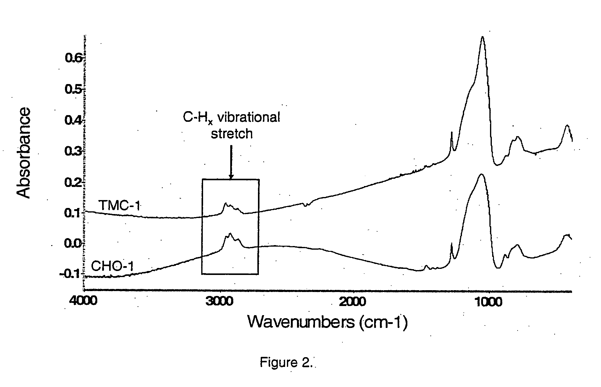
[0143]FIG. 4 shows the FT-IR spectra of the DEMS / CHO fil...


PUM

PropertyMeasurementUnit
Temperatureaaaaaaaaaa
Fractionaaaaaaaaaa
Fractionaaaaaaaaaa

Abstract

A porous organosilicate glass (OSG) film: SivOwCxHyFz, where v+w+x+y+z=100%, v is 10 to 35 atomic %, w is 10 to 65 atomic %, x is 5 to 30 atomic %, y is 10 to 50 atomic % and z is 0 to 15 atomic %, has a silicate network with carbon bonds as methyl groups (Si—CH3) and contains pores with diameter less than 3 nm equivalent spherical diameter and dielectric constant less than 2.7. A preliminary film is deposited by a chemical vapor deposition method from organosilane and/or organosiloxane precursors, and independent pore-forming precursors. Porogen precursors form pores within the preliminary film and are subsequently removed to provide the porous film. Compositions, film forming kits, include organosilane and/or organosiloxane compounds containing at least one Si—H bond and porogen precursors of hydrocarbons containing alcohol, ether, carbonyl, carboxylic acid, ester, nitro, primary amine, secondary amine, and/or tertiary amine functionality or combinations.

Description

CROSS-REFERENCE TO RELATED APPLICATIONS [0001] This application claims the benefit of U.S. Provisional Application No. 60 / 613,937, filed 28 Sep. 2004.BACKGROUND OF THE INVENTION [0002] Low dielectric constant materials produced by chemical vapor deposition (CVD) methods are typically used as insulating layers in electronic devices. The electronics industry uses dielectric materials as insulating layers between circuits and components of integrated circuits (IC) and associated electronic devices. Line dimensions are being reduced in order to increase the speed and device density of microelectronic devices (e.g. computer chips). As the line dimensions decrease, the insulating requirements for the interlayer dielectric (ILD) become more rigorous. Shrinking the spacing requires a lower dielectric constant to minimize the RC time constant, where R is the resistance of the conductive line and C is the capacitance of the insulating dielectric interlayer. C is inversely proportional to spac...

Claims


Application Information

Patent Timeline
IPC IPC(8): C23C16/00B32B17/06B32B13/04B32B9/00B32B19/00
CPCC03C3/045C23C16/30C23C16/401C23C16/56H01L21/02126H01L21/02203H01L21/02274H01L21/02348H01L21/3105H01L21/3122H01L21/31695Y10T428/31663
Inventor LUKAS, AARON SCOTTO'NEILL, MARK LEONARDKARWACKI, EUGENE JOSEPH JR.VRTIS, RAYMOND NICHOLASVINCENT, JEAN LOUISE
Owner VERSUM MATERIALS US LLC
Why Eureka
Try Eureka