Method for applying metal features onto metallized layers using electrochemical deposition

Inactive Publication Date: 2006-04-13
SEMITOOL INC
View PDF25 Cites 2 Cited by
  • Summary
  • Abstract
  • Description
  • Claims
  • Application Information

AI Technical Summary

Benefits of technology

[0019] The processes of the present invention provide an attractive alternative to processes that deposit seed layers using PVD or CVD. By avoiding the costs associated with PVD and CVD, integrated circuit manufacturers will be able to produce their products more cost-effectively. The present invention will also allow integrated circuit manufacturers to increase their throughput by avoiding time-cons

Problems solved by technology

Despite the advantages of copper, it has not been as widely used as an interconnect material as one would expect.
This is due, at least in part, to the difficulty in effectively and economically depositing copper metallization.
Unfortunately, materials used as barrier layers typically do not exhibit the electrical conductive properties necessary to allow for the uniform electrochemical deposition of copper directly onto the barrier layers using conventional gap fill chemistries and processes.
CVD can result in conformal copper coverage over a variety of topological profiles; however, CVD is expensive to carry out and utilizes expensive eq

Method used


Image

  • Method for applying metal features onto metallized layers using electrochemical deposition
  • Method for applying metal features onto metallized layers using electrochemical deposition
  • Method for applying metal features onto metallized layers using electrochemical deposition

Examples


Example

EXAMPLE 1

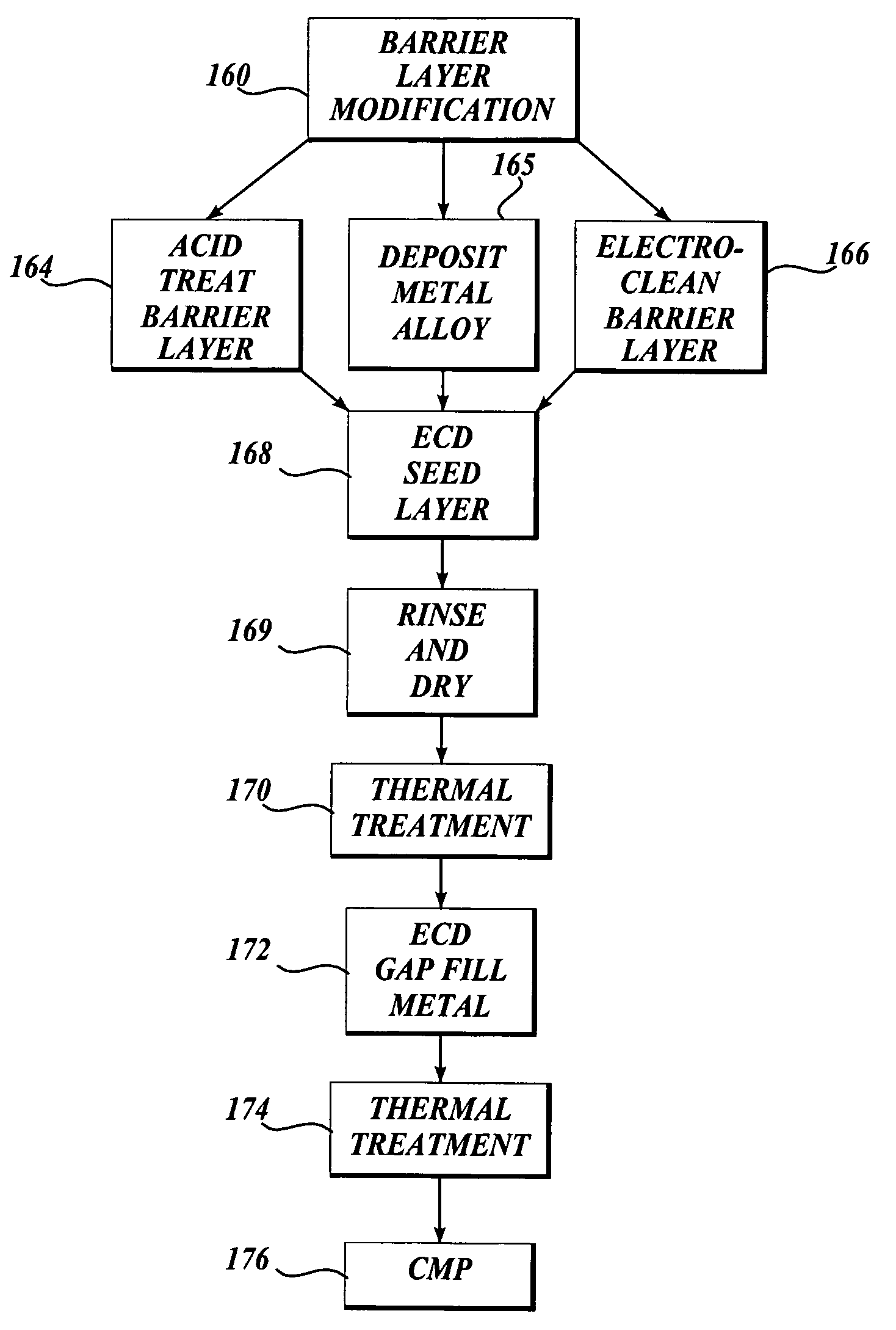
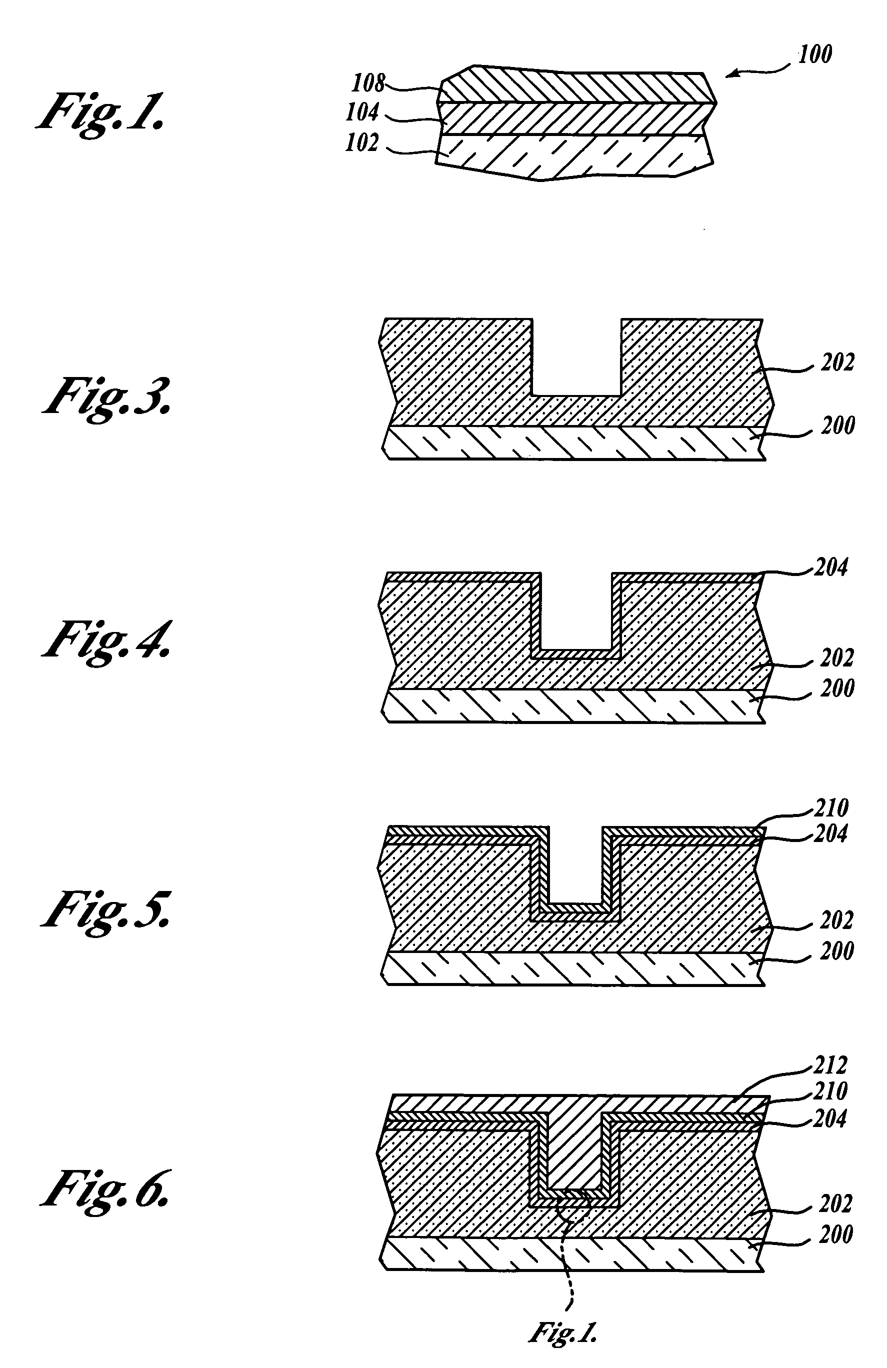
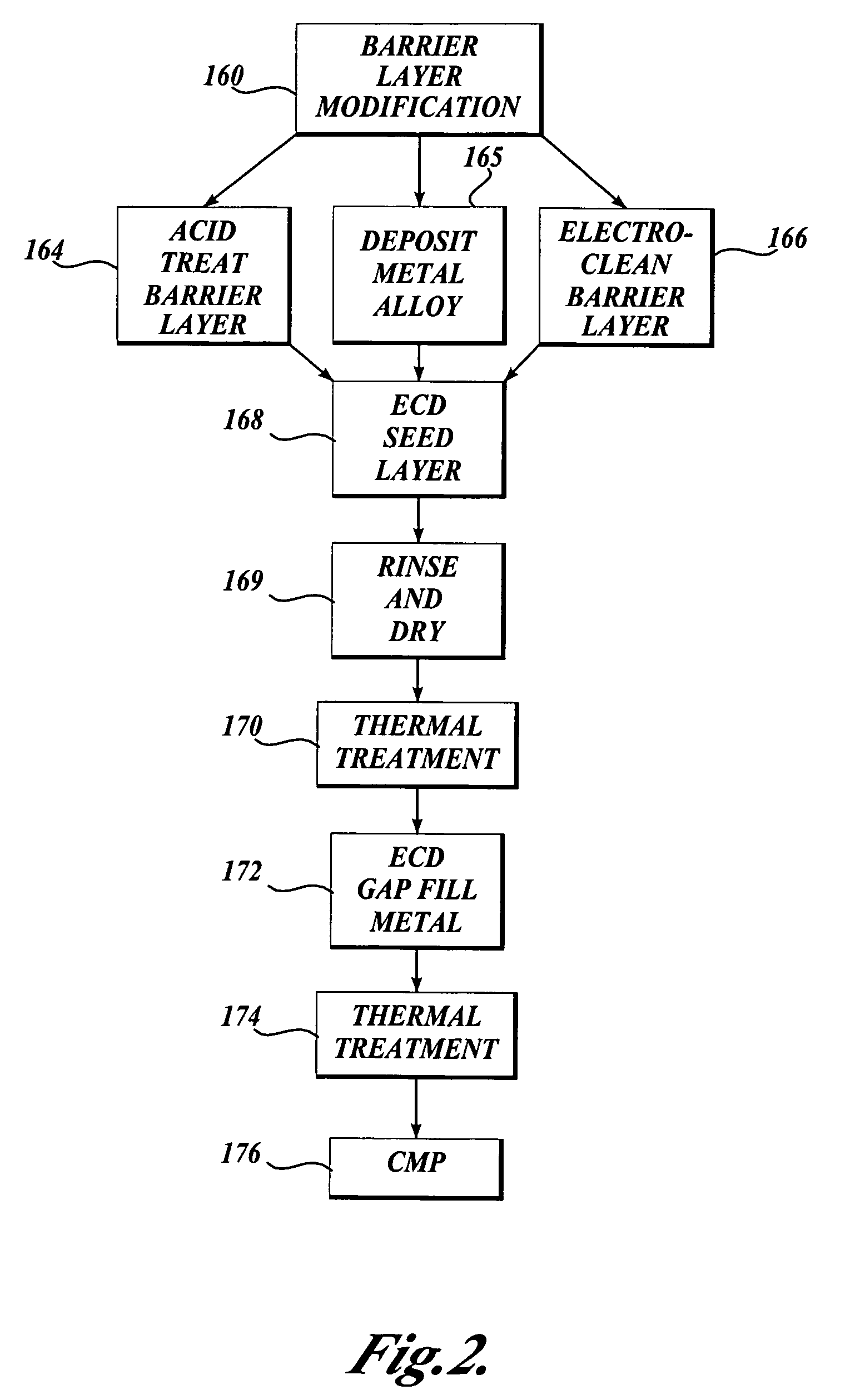
[0096] Acid Treatment of Barrier Layer.

[0097] Acid treatment of a tantalum barrier was performed using 2% by weight aqueous solution of hydrofluoric acid. A 200 mm blanket wafer deposited with 25 nanometers of PVD tantalum barrier was used. This rotating wafer was subjected to a water spray treatment for 15 seconds followed by an acid spray treatment for 15 seconds. Then the rotating wafer was cleaned by spraying de-ionized water for another 15 seconds to remove the excess acid from its surface. For an additional 5 seconds, the wafer was rotated to sling off large water droplets. The wafer was then wet-transferred to a plating chamber. In the plating chamber, the wafer was plated with copper up to a thickness of ˜80 nanometers. After plating, the wafer was cleaned insitu with de-ionized water and the wafer was transferred to a SRD (Spin, Rinse, and Dry) chamber. In this SRD chamber, the spinning wafer was once again cleaned with de-ionized water thoroughly to remove any p...

Example

EXAMPLE 2

[0098] Electrolytic Treatment of Barrier Layer.

[0099] Electrolytic treatment of a tantalum barrier was performed using 2% by weight of potassium hydroxide aqueous solution. A 200 mm blanket wafer with 25 nanometers of PVD tantalum barrier was treated. This rotating wafer was used as a cathode and subjected to a current of 1 A (˜3 mA / cm2) for one minute while an inert platinum electrode was the anode. The wafer was then wet-transferred to a SRD chamber where the spinning wafer was rinsed with de-ionized water and then once again wet transferred to a plating chamber. In the plating chamber, the wafer was plated with copper up to a thickness of about 80 nanometers. After plating, the wafer was cleaned insitu with de-ionized water and the wafer was transferred to a SRD chamber. In this SRD chamber, the spinning wafer was once again cleaned with de-ionized water thoroughly to remove any plating chemistry left on its surface. After rinsing, the wafer was dried by spinning it in...


PUM

PropertyMeasurementUnit
Percent by massaaaaaaaaaa
Adhesion strengthaaaaaaaaaa

Abstract

The present invention is directed to a process for producing structures containing metallized features for use in microelectronic workpieces. The process treats a barrier layer to promote the adhesion between the barrier layer and the metallized feature. Suitable means for promoting adhesion between barrier layers and metallized features according to the invention include an acid treatment of the barrier layer, an electrolytic treatment of the barrier layer, or deposition of a bonding layer between the barrier layer and metallized feature. The present invention thus modifies an exterior surface of a barrier layer making it more suitable for electrodeposition of metal on a barrier, thus eliminating the need for a PVD or CVD seed layer deposition process.

Description

CROSS-REFERENCE TO RELATED APPLICATION [0001] This application is a continuation of U.S. application Ser. No. 10 / 470,287, filed Jul. 22, 2003, which is the National Stage of International Application No. PCT / US03 / 00890, filed Jan. 10, 2003, which claims the benefit of U.S. Application No. 60 / 347,520, filed Jan. 10, 2002.FIELD OF THE INVENTION [0002] The present invention is directed to methods for forming metallized structures on barrier layers through electrochemical deposition. BACKGROUND OF THE INVENTION [0003] In the fabrication of microelectronic devices, application of one or more metallization layers is an important step in the overall fabrication process. The metallization may be used in the formation of discrete microelectronic components, but is most often used to provide interconnect components formed on a workpiece, such as a semiconductor wafer. For example, metallized structures are used to interconnect devices of an integrated circuit. [0004] An integrated circuit is ...

Claims


Application Information

Patent Timeline
IPC IPC(8): C25D5/34H01L21/44C23C18/18C25D3/38C25D5/18C25D5/38C25D5/54C25D7/12H01L21/288H01L21/321H01L21/3213H01L21/4763H01L21/768
CPCC25D3/38C25D5/18C25D5/34C25D5/38C25D5/54H01L21/2885H01L21/321H01L21/32134H01L21/76843H01L21/76846H01L21/76861H01L21/76864H01L21/76873H01L21/76885H01L2221/1089C23C18/1605C25D7/123C25D5/627
Inventor BASKARAN, RAJESHKIM, BIOHCHEN, LINLINGRAHAM, LYNDON W.
Owner SEMITOOL INC
Why Eureka
Try Eureka