

Method for producing photonic crystal and photonic crystal
- Summary
- Abstract
- Description
- Claims
- Application Information
AI Technical Summary
Benefits of technology
Problems solved by technology
Method used
Image

Examples
first embodiment
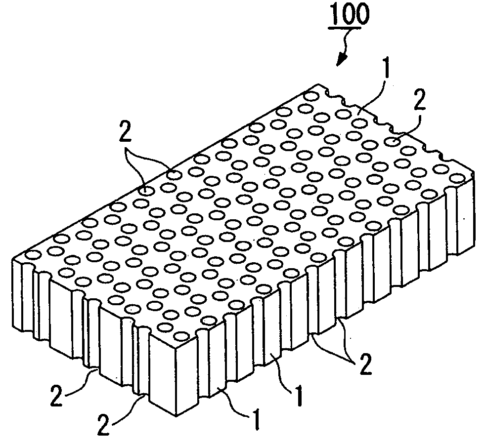
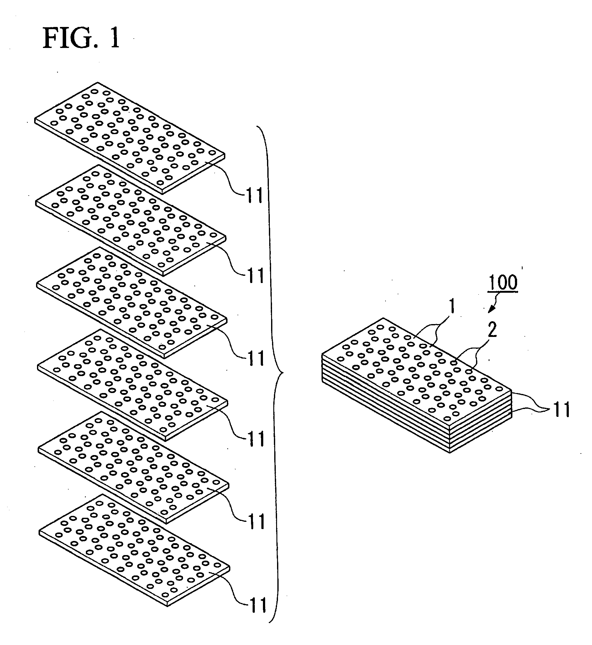
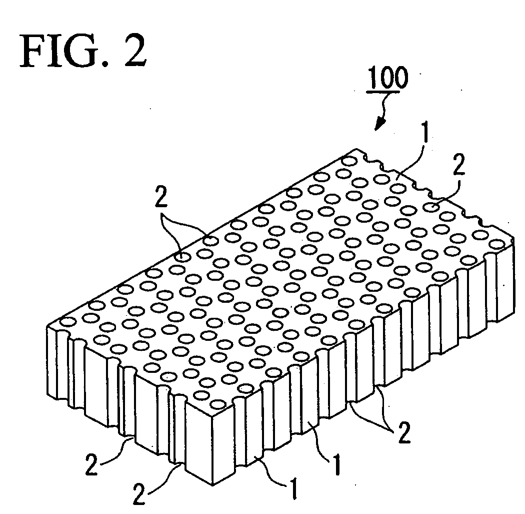
[0066]FIG. 2 is a perspective view illustrating a photonic crystal in the first embodiment.
[0067] The photonic crystal 100 includes a first dielectric portion 1 and second dielectric portions 2. The photonic crystal 100 has a two-dimensional periodic structure, and the second dielectric portions 2 are arrayed so as to penetrate from the front surface to the back surface of the photonic crystal 100.
[0068] In the photonic crystal 100 in the first embodiment, a dielectric ceramic constitutes the first dielectric portion 1 and air as a dielectric constitutes the second dielectric portions 2.
[0069] The dielectric ceramic constituting the first dielectric portion 1 is larger in relative dielectric constant than dielectrics used in semiconductor technology such as Si and GaAs, polymer materials and photo curable resins, and downsizing of elements is thereby made possible. This is because the wavelength in a dielectric is inversely proportional to the square root of the relative dielectr...
second embodiment
[0080]FIG. 4 is a perspective view illustrating a photonic crystal in the second embodiment.
[0081] As shown in FIG. 4, a photonic crystal 100A includes a first dielectric portion 1A and second dielectric portions 2A. The first dielectric portion 1A is constituted with a first dielectric ceramic and the second dielectric portions 2A are constituted with a second dielectric ceramic. The photonic crystal 100A has a two-dimensional periodic structure, and the second dielectric portions 2A penetrate from the front surface to the back surface of the photonic crystal 10A.
[0082] The photonic crystal 100A of the second embodiment is characterized by using a dielectric ceramic for each of the first dielectric portion 1A and the second dielectric portions 2A. By using two dielectric ceramics, there can be obtained a photonic crystal 100A having a high strength and excellent properties, making downsizing of elements possible.
[0083] According to the properties demanded for the photonic crysta...
example 1
[0248] On the basis of the flowchart shown in FIG. 8, hole-perforated sheets were laminated, and then a photonic crystal 100A was produced by filling the dielectric sheets.
[0249] As a first dielectric ceramic, a BaO—SiO2—Al2O3—B2O3 based powder (dielectric constant: 6.4) having a mean particle size of 0.7 μm was prepared. As a second dielectric ceramic, a BaO—Nd2O3—TiO2—B2O3—ZnO2—CuO based powder (dielectric constant: 75.4) having a mean particle size of 1.0 μm was prepared.
[0250] At the beginning, the first dielectric ceramic, a dispersant, a resin and a dispersion medium were mixed together by use of a ball mill, to yield a slurry. Then, by use of a doctor-blade method, the slurry was converted into a sheet to prepare a 82 mm×82 mm×120 μm green sheet. The proportions of the first dielectric ceramic, the resin and the dispersion medium were set at 23:11:66 by vol %. The types of the dispersant, resin and dispersion medium and the addition amount of the dispersant were as follows:...
PUM
 Abstract
Description
Claims
Application Information