Light emitting device using nitride semiconductor and fabrication method of the same

a light emitting device and nitride technology, applied in semiconductor/solid-state device manufacturing, semiconductor devices, semiconductors, etc., can solve the problems of reducing the luminous efficiency of the nitride based 3-5 group compound semiconductor light emitting device, the reliability of the light emitting device is affected, etc., to improve the performance and reliability of the light emitting device, improve the crystallinity of the gan based single crystal layer, and reduce the defect of the single crystal

Active Publication Date: 2006-04-20
SUZHOU LEKIN SEMICON CO LTD
View PDF6 Cites 20 Cited by
  • Summary
  • Abstract
  • Description
  • Claims
  • Application Information

AI Technical Summary

Benefits of technology

[0014] The advantage of the present invention is to reduce crystal defects of a GaN based single crystal layer as well as improve its crystallinity, thereby improving the performance and reliability thereof.
[0015] As another advantage, the present invention can practically realize high brightness performance from an active layer of only a single quantum well structure.

Problems solved by technology

As a result, this degrades electrical characteristics of the nitride based 3-5 group compound semiconductor light emitting device, and more particularly, increases leakage current under reverse bias conditions, thereby causing a fatal effect to the reliability of the light emitting device.
In addition, the crystal defects created in the interface between the substrate and the buffer layer degrades the crystallinity of the active layer, and therefore disadvantageously lowers the luminous efficiency of the nitride based 3-5 group compound semiconductor light emitting device.

Method used


Image

  • Light emitting device using nitride semiconductor and fabrication method of the same
  • Light emitting device using nitride semiconductor and fabrication method of the same
  • Light emitting device using nitride semiconductor and fabrication method of the same

Examples


first embodiment

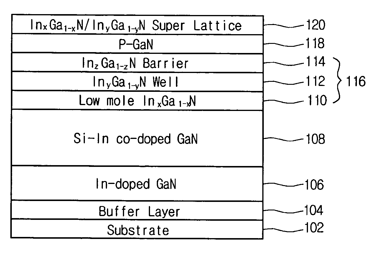
[0022]FIG. 1 illustrates a structure of a nitride based 3-5 group compound semiconductor light emitting device according to a first embodiment of the present invention.

[0023] As shown in FIG. 1, a nitride based 3-5 group compound semiconductor light emitting device has a cross-sectional structure including a buffer layer 104 grown on a substrate 102, a first electrode contact layer 108 made of an n-type GaN layer (codoped with Si and In) and a second electrode contact layer 120 of an InxGa1−xN / InyGa1−yN super lattice structure. Herein, the first and second electrode contact layers 108 and 120 are provided with electrodes (not shown), respectively, in following process steps so that external voltage can be applied thereto via the electrodes.

[0024] The nitride based 3-5 group compound semiconductor light emitting device of the present invention also has an active layer 116 of a quantum well structure which is interposed between the first electrode contact layer 108 and the second el...

second embodiment

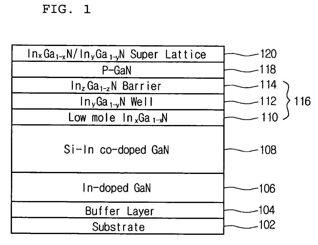
[0041]FIG. 2 illustrates a structure of a nitride based 3-5 group compound semiconductor light emitting device according to a second embodiment of the present invention.

[0042] The structure of the nitride based 3-5 group compound semiconductor light emitting device of this embodiment shown in FIG. 2 is basically similar to that of the first embodiment except that an InxGa1−xN / InyGa1−yN super lattice structure layer 210 is additionally placed underlying a first electrode contact layer 212 forming a heterostructure in order to minimize crystal defects originated from the mismatch of lattice constant and thermal expansion coefficient between a substrate 202 and a Si / In-doped GaN based single crystal layer 212.

[0043] This structure can reduce dislocation density propagated from the substrate 202 and a low temperature buffer layer 204 to improve the reverse breakdown voltage Vbr of the light emitting device thereby improving the reliability thereof.

[0044] The structure of the nitride ...

third embodiment

[0050]FIG. 3 illustrates a structure of a nitride based 3-5 group compound semiconductor light emitting device according to a third embodiment of the present invention.

[0051] Referring to FIG. 3, this embodiment is generally similar to the first embodiment except that an In-doped GaN layer 318 is additionally interposed between a p-type GaN layer 320 and an InzGa1−zN barrier layer 314 to form a heterostructure.

[0052] The additional In-doped GaN layer 318 can restrain the in-diffusion of Mg atoms used as dopant in the p-type GaN layer 320 thereby improving characteristics. The In-doped GaN layer 318 is grown to a thickness of 100 Å or less.

[0053] Hereinafter a fabrication method of the semiconductor light emitting device of the third embodiment will be described. A buffer layer 304 is grown on a substrate 302, a first electrode contact layer 308 is made of an n-type GaN (codoped with Si and In), and a second electrode contact layer 322 is formed of an InxGa1−xN / InyGa1−yN super lat...


PUM


Abstract

A nitride based 3-5 group compound semiconductor light emitting device comprising: a substrate; a buffer layer formed above the substrate; a first In-doped GaN layer formed above the buffer layer; an InxGa1−xN / InyGa1−yN super lattice structure layer formed above the first In-doped GaN layer; a first electrode contact layer formed above the InxGa1−xN / InyGa1−yN super lattice structure layer; an active layer formed above the first electrode contact layer and functioning to emit light; a second In-doped GaN layer; a GaN layer formed above the second In-doped GaN layer; and a second electrode contact layer formed above the GaN layer. The present invention can reduce crystal defects of the nitride based 3-5 group compound semiconductor light emitting device and improve the crystallinity of a GaN GaN based single crystal layer in order to improve the performance of the light emitting device and ensure the reliability thereof.

Description

[0001] This application is a Divisional of co-pending application Ser. No. 10 / 517,819, filed on Dec. 14, 2004, and for which priority is claimed under 35 U.S.C. § 120. Application Ser. No. 10 / 517,819 is the national phase of PCT International Application No. PCT / KR2004 / 001480 filed on Jun. 21, 2004 under 35 U.S.C. § 371, which claims priority on Korean Application No. 41409 / 2003 filed in Korea on Jun. 25, 2003. The entire contents of each of the above-identified applications are hereby incorporated by reference.TECHNICAL FIELD [0002] The present invention relates to a nitride based 3-5 group compound semiconductor. More particularly, the present invention relates to a nitride based 3-5 group compound semiconductor light emitting device and a fabrication method thereof capable of reducing crystal defects originated from the mismatch of thermal expansion coefficient and lattice constant between a substrate and a GaN based single crystal layer grown thereon as well as improving the cry...

Claims


Application Information

Patent Timeline
Patent Type & Authority Applications(United States)
IPC IPC(8): H01L29/06H01L33/06H01L33/12H01L33/32
CPCH01L33/04H01L33/12H01L33/32
Inventor LEE, SUK HUN
Owner SUZHOU LEKIN SEMICON CO LTD
Why Eureka
Try Eureka