Semiconductor device having misfet using high dielectric constant gate insulation film and method for fabricating the same

Inactive Publication Date: 2006-04-20
KK TOSHIBA
View PDF6 Cites 88 Cited by
  • Summary
  • Abstract
  • Description
  • Claims
  • Application Information

AI Technical Summary

Benefits of technology

[0027]FIG. 6 is a graph showing a plot of electron mobility vs. effective gate field intensity for explanation of effects of the embodiment 1.
[0028]FIG. 7 is a graph showing a plot of hole mobility vs. effective gate field intensity for explanation of effects of the embodiment 1.
[0029]FIG. 8 is a graph showing flat-band voltages for explanation of effects of the embodiment 1.
[0030]FIG. 9 is a graph showin

Problems solved by technology

Unfortunately, using such ultrathin SiO2 film as a gate insulator film results in a gate leakage current due to “tunnel” currents reaching a non-negligible value with respect to source/drain currents.
This poses a serious problem that impedes accomplishment of both increased current driving ability or “drivability” and reduced power consumption.
Additionally, in the case of using the EOT-reduced gate insulator film, when using a polycrystalline silicon or “poly-silicon” layer for the gate electrode, a problem takes place as to the so-called depletion—that is, a depleted layer can be formed in a polysilicon layer region with a contact between the gate electrode and the gate insulator film.
This depletion badly behaves to increase the effective thickness of the gate insulator film.
However, in the prior art MISFET device having the aforesaid high dielectric gate insulation film (high-k gate insulator film), charge carriers such as electrons or holes decrease in mobility.
As shown in FIG. 14, the use of the high-k gate insulator film results i

Method used


Image

  • Semiconductor device having misfet using high dielectric constant gate insulation film and method for fabricating the same
  • Semiconductor device having misfet using high dielectric constant gate insulation film and method for fabricating the same
  • Semiconductor device having misfet using high dielectric constant gate insulation film and method for fabricating the same

Examples


embodiment 1

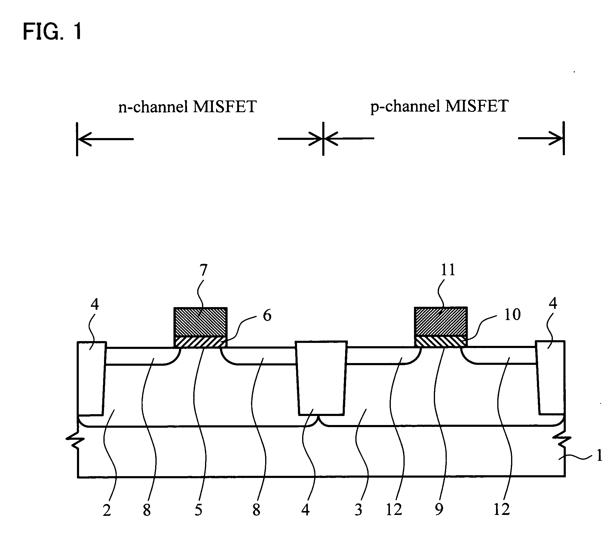
[0039] Referring to FIG. 1, there is shown a cross-sectional view of a complementary metal insulator semiconductor field effect transistor (MISFET) device having an n-channel MISFET and a p-channel MISFET in accordance with an embodiment 1 of this invention, wherein each MISFET has a high dielectric material gate insulation film and a gate electrode of the flat structure.

[0040] As shown in FIG. 1, a silicon substrate 1 has its top surface portion, in which a p-type well layer 2 and an n-type well layer 3 are formed. And, active regions of the n- and p-channel MISFETs are partitioned by a pattern of element isolation region 4 as formed by known shallow trench isolation (STI) techniques. In the active region of the n-channel MISFET, an n-channel interface layer 5 is formed at its channel surface, on which a patterned n-channel high dielectric material gate insulation film 6 and an n-channel gate electrode 7 are stacked with a pair of spaced-apart n-type source / drain diffusion layers ...

embodiment 2

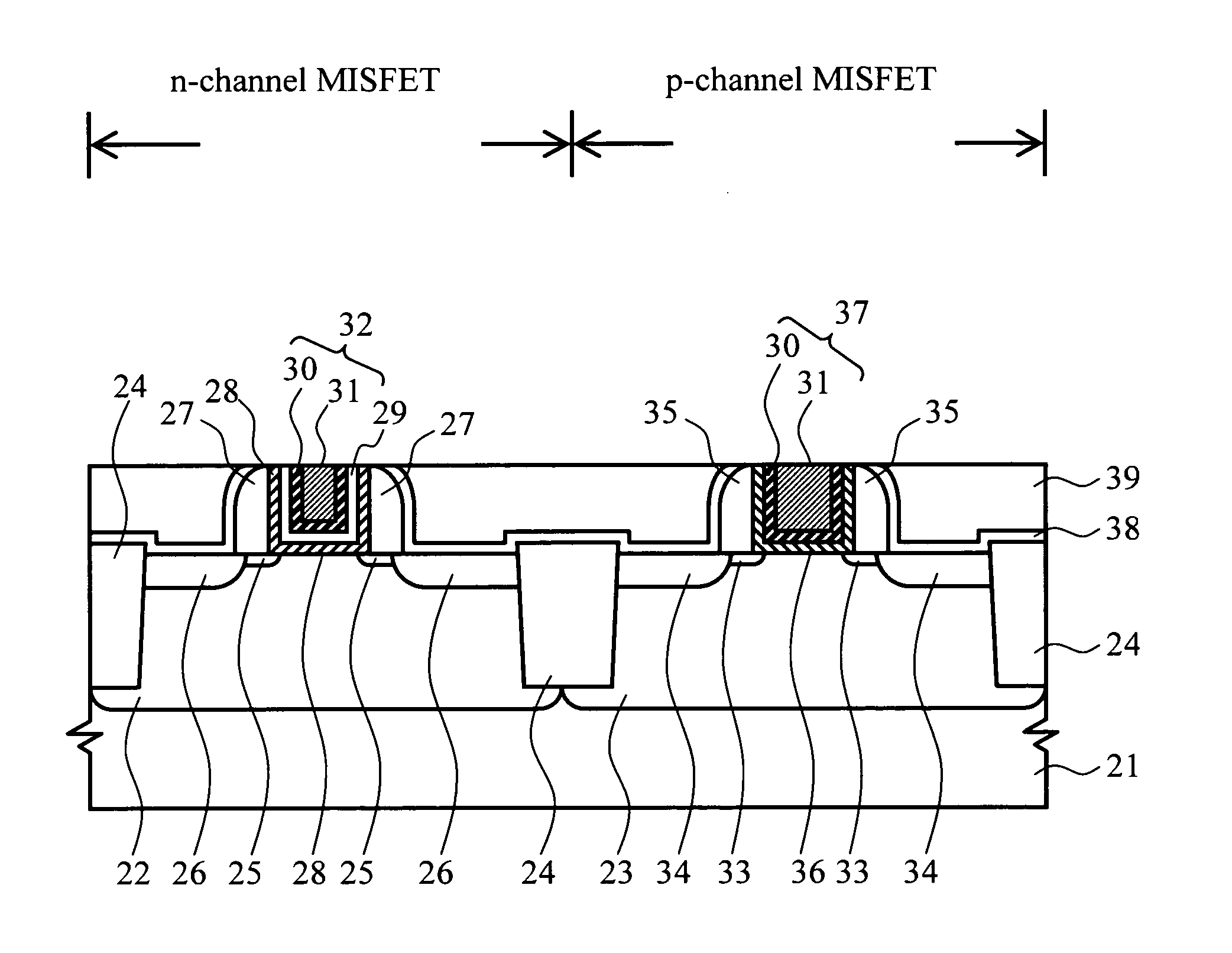
[0068] An explanation will next be given of a case where this invention is applied to a MISFET device of the type having a damascene gate electrode structure with reference to FIGS. 10, 11A-11J and 12 below. FIG. 10 illustrates, in cross-section, a complementary MISFET device incorporating the principles of the invention, and FIGS. 11A-11J depict in cross-section some major steps in the manufacture of the device. FIG. 12 is a sectional view of a modified example of the MISFET device, also embodying the invention.

[0069] As shown in FIG. 10, a silicon substrate 21 has its top surface in which a p-well layer 22 and an n-well layer 23 are formed. Active region of an n-channel MISFET and n-channel MISFET are partitioned by an STI element isolation layer 23. In the n-channel MISFET active region, a pair of laterally opposing n-type extension layers 25 and a pair of n-type source / drain diffusion layers 26 are formed so that each extension is coupled to its associated diffusion. At upper p...


PUM


Abstract

A semiconductor device having a metal insulator semiconductor field effect transistor (MISFET) with increased electron mobility and enhanced hole mobility is disclosed. In this semiconductor device, a p-type well layer and an n-type well layer are formed in a surface portion of a silicon substrate. A nitrogen-nondoped n-channel interface layer and a nitrogen-free n-channel high dielectric constant gate insulation film plus an n-channel gate electrode are formed in an n-channel MISFET as partitioned by an element isolation region. And, n-type source/drain diffusion layers are provided. In a p-channel MISFET, a nitrogen-doped p-channel interface layer, a nitrogen-added p-channel high dielectric gate insulation film and a p-channel gate electrode are formed along with p-channel source/drain diffusion layers as provided therein. A method of fabricating this semiconductor device is also disclosed.

Description

CROSS-REFERENCE TO RELATED APPLICATIONS [0001] This application is based on and claims priority of Japanese Patent Application (JPA) No. 2004-263784, filed on Sep. 10, 2004 and also JPA No. 2004-354791, filed Dec. 8, 2004, the entire contents of which are incorporated herein by reference. FIELD OF THE INVENTION [0002] The present invention relates generally to semiconductor devices having metal insulator semiconductor field effect transistors (MISFETs) using a high dielectric constant gate insulating film and methodology of making the same. More particularly but not exclusively, this invention relates to a semiconductor device having n-channel and p-channel MISFETs with a high dielectric constant (high-k) film applied as a gate insulation film used for insulated-gate FETs (MISFETs) and a fabrication method thereof. DESCRIPTION OF RELATED ART [0003] In recent years, diligent efforts are made to achieve further miniaturization and higher integration of semiconductor devices, in partic...

Claims


Application Information

Patent Timeline
IPC IPC(8): H01L29/76
CPCH01L21/28088H01L21/823842H01L21/823857H01L29/4958H01L29/4966H01L29/517H01L29/7833
Inventor AKASAKA, YASUSHIMIYAGAWA, KAZUHIROSASAKI, TAKAOKI
Owner KK TOSHIBA
Why Eureka
Try Eureka